· AtlasPCB Engineering · Engineering · 16 min read
HDI Via Reliability Under Thermal Cycling: Testing, Failure Modes & Design Guidelines
Learn how HDI microvias perform under thermal cycling stress. Explore failure mechanisms, IPC testing standards, and design strategies for maximum via reliability.

HDI microvias are the backbone of modern high-density PCB designs — enabling [fine-pitch BGA escape routing]/blog/hdi-pcb-design-guide/), compact form factors, and multi-gigabit signal paths. But every microvia is a potential reliability risk when the board is subjected to thermal cycling. The repeated expansion and contraction of copper and dielectric materials generates cumulative stress that eventually causes electrical failure.
Understanding how and why HDI vias fail under thermal cycling is essential for any designer or engineer specifying boards for automotive, aerospace, medical, or industrial applications where field life extends to 15–20 years and thousands of temperature excursions.
This article examines the physics behind microvia failure, the IPC test methods used to qualify via reliability, how different via structures compare, and the design and manufacturing choices that separate a 200-cycle failure from a 1,000+ cycle survivor.
Why Thermal Cycling Matters for HDI Vias
The CTE Mismatch Problem
Every PCB is a composite of materials with different coefficients of thermal expansion (CTE). Copper expands at approximately 17 ppm/°C. FR-4 and other common dielectric materials expand at 14–18 ppm/°C in the X-Y plane — reasonably matched to copper — but at 40–70 ppm/°C in the Z-axis (through-thickness direction) before the glass transition temperature (Tg), and even higher above Tg.
This Z-axis CTE mismatch is the fundamental driver of via failure. During heating, the dielectric expands far more than the copper barrel in the through-thickness direction, stretching the copper wall of the via. During cooling, it contracts. Each cycle accumulates plastic strain in the copper, eventually nucleating cracks that propagate to full electrical opens.
For [HDI microvias]/blog/hdi-pcb-technology/), the geometry makes this problem both better and worse than traditional through-hole vias:
- Better: Microvias span only one or two dielectric layers (typically 60–100 µm each), so the absolute Z-axis displacement per cycle is small.
- Worse: Microvias are laser-drilled with tapered profiles and thin copper plating (typically 15–25 µm), leaving less copper to absorb strain. The bottom connection (target pad interface) creates a geometric stress concentrator.
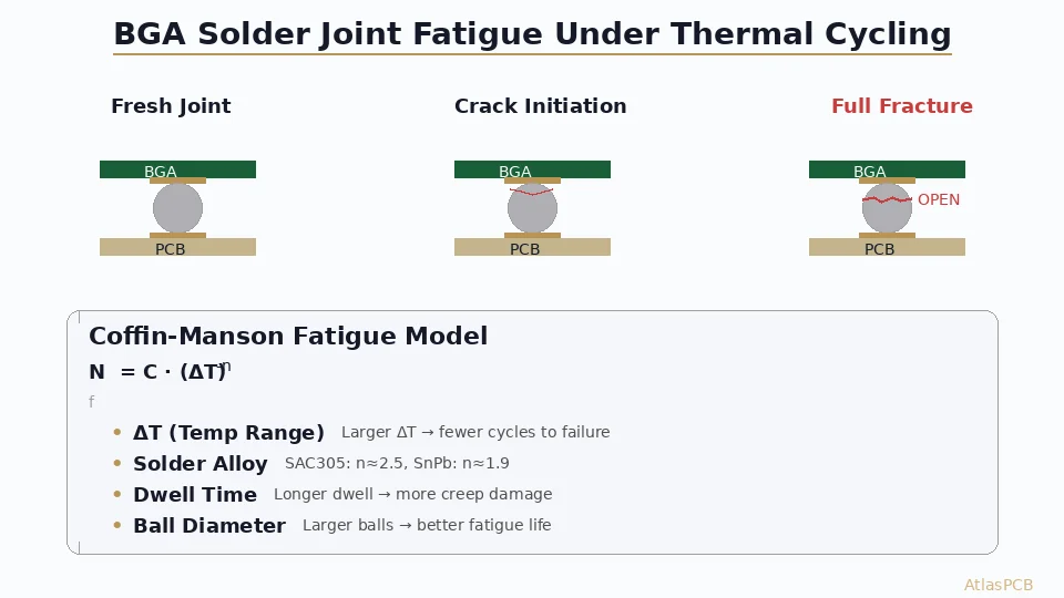
Cumulative Damage and the Fatigue Curve
Microvia failure under thermal cycling follows classic low-cycle fatigue behavior. The copper plating does not fail on the first cycle — it accumulates plastic deformation over hundreds or thousands of cycles until a crack initiates. Once a crack forms, it propagates rapidly, and resistance climbs exponentially.
The relationship follows a Coffin-Manson model: cycles to failure (Nf) is inversely proportional to the plastic strain range raised to a power. This means that wider temperature swings dramatically reduce cycle life — a via that survives 2,000 cycles from 0°C to 100°C may fail in 500 cycles from -55°C to +125°C.
Failure Mechanisms in HDI Microvias
Understanding the specific failure modes is critical for both design prevention and failure analysis. The three primary mechanisms each originate from different locations within the via structure.
Barrel Cracking
Barrel cracking occurs in the copper plating along the sidewall of the via. As the dielectric expands in the Z-axis, it stretches the copper barrel beyond its elastic limit. Cracks typically initiate at the thinnest point of the plating — often near the midpoint of the via barrel or at locations where plating thickness is non-uniform.
Key factors accelerating barrel cracking:
- Plating thickness below 18 µm (IPC-6012 minimum for Class 3 is 20 µm for through-hole vias; microvias have different criteria)
- High aspect ratio vias where plating uniformity is difficult to achieve
- Dielectric materials with high Z-axis CTE, especially above Tg
- Plating voids or inclusions that act as crack nucleation sites
In cross-section analysis, barrel cracks appear as circumferential fractures in the copper sidewall. They may be partial (reducing cross-section and increasing resistance) or complete (open circuit).
Interfacial Separation (Target Pad Failure)
This is the most common failure mode in HDI microvias, particularly stacked structures. The interface between the bottom of the microvia and the target pad (the capture pad on the underlying layer) experiences a complex stress state during thermal cycling.
The failure occurs because:
- The microvia copper connects to the target pad at a near-perpendicular angle, creating a stress concentration.
- The copper-to-copper bond at this interface depends on plating quality — specifically, the nucleation and adhesion of the electroplated copper onto the target pad surface.
- Any contamination, oxide layer, or plating chemistry residue at the target pad surface before microvia plating weakens this bond.
- In stacked via configurations, the lower via’s target pad is simultaneously the upper via’s barrel bottom, creating compound stress.
Cross-sectional failure analysis reveals a clean separation at the target pad interface — the microvia copper lifts away from the pad below. This mode is sometimes called “pad cratering” when it involves fracture within the dielectric beneath the pad, though true interfacial separation is a copper-to-copper bond failure.
Corner Cracking in Stacked Vias
When [microvias are stacked]/blog/pcb-via-types-guide/) (one directly on top of another), the junction between the upper via and the lower via creates geometric stress concentration at the corners. The transition from vertical barrel to horizontal pad to vertical barrel below concentrates strain at the inner and outer corners of this junction.
Corner cracking is particularly insidious because:
- It affects the most space-efficient via structure (stacked vias) that designers prefer for dense BGA routing
- Cracks may initiate internally and not be visible on surface inspection
- The failure is progressive — initial corner cracks may not cause immediate opens but degrade resistance over time
- Unfilled or partially filled vias dramatically increase corner crack susceptibility because the void creates a free surface for crack propagation
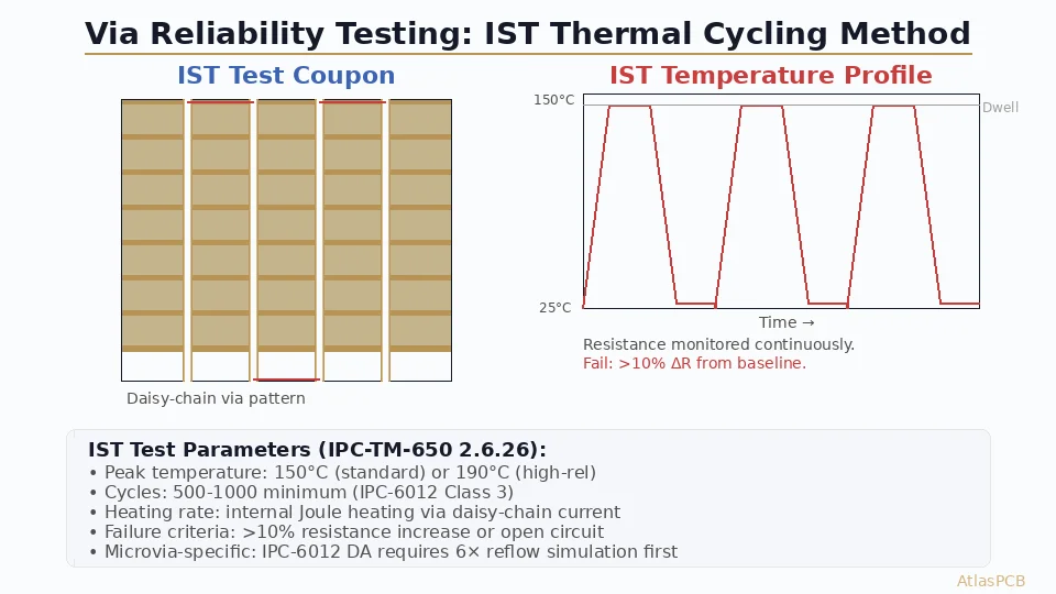
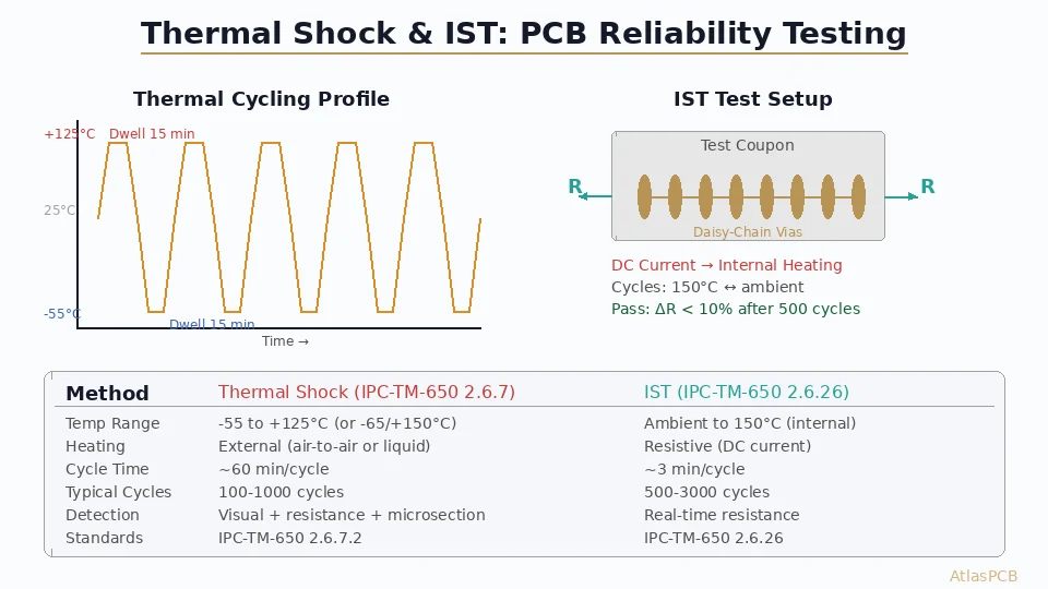
IPC Testing Standards for Via Reliability
IPC-TM-650 Method 2.6.26: Thermal Cycling
This is the primary test method for evaluating interconnect stress resistance under thermal cycling. The test specification defines:
- Temperature range: -55°C to +125°C (for most qualification programs)
- Dwell time: Minimum 10 minutes at each temperature extreme (sufficient for the test coupon to reach thermal equilibrium)
- Transfer time: Maximum 2 minutes between temperature extremes (for liquid-to-liquid thermal shock) or as defined for air-to-air cycling
- Number of cycles: Determined by the applicable performance specification (IPC-6012, IPC-6018, etc.)
- Pass/fail criterion: Resistance increase ≤ 10% from baseline for continuity circuits
The test uses dedicated test coupons — typically daisy-chain patterns that series-connect multiple vias so that a single via failure produces a measurable resistance change. Resistance is monitored either continuously (in-situ) or at defined intervals.
IPC-TM-650 Method 2.6.27: Thermal Stress (Solder Float)
While not a cycling test, the solder float test per Method 2.6.27 is a complementary assessment. Test coupons are floated on molten solder at 288°C for 10 seconds (simulating a worst-case reflow excursion). The rapid thermal exposure stresses vias through a single extreme event rather than cumulative cycling.
This test is particularly relevant for detecting manufacturing defects (poor plating adhesion, voids) that would eventually cause cycling failures but might not show up until hundreds of cycles.
IPC-6012: Qualification Requirements by Class
[IPC-6012]/blog/pcb-reliability-testing/) defines three performance classes with different via reliability requirements:
| Parameter | Class 1 (General) | Class 2 (Dedicated Service) | Class 3 (High Reliability) |
|---|---|---|---|
| Thermal cycling range | Per end-use specification | -25°C to +125°C typical | -55°C to +125°C |
| Minimum cycles | Application-dependent | 100–200 | 300+ |
| Max resistance change | ≤ 10% | ≤ 10% | ≤ 10% |
| Solder float (288°C) | 3 cycles | 4 cycles | 6 cycles |
| Microvia plating thickness | 12 µm min | 18 µm min | 20 µm min |
For applications beyond Class 3 — such as space (IPC-6012ES), military (IPC-6012DS), or automotive (IPC-6012DA) — additional cycling requirements and tighter acceptance criteria apply. Automotive qualification per AEC-Q100 board-level reliability often specifies 1,000 cycles at -40°C to +125°C.
IST (Interconnect Stress Testing)
IST is an accelerated reliability test method that uses internal resistive heating of the PCB coupon rather than an external thermal chamber. A current-induced temperature cycle (typically ambient to 150°C) can complete in 3–4 minutes versus the 30–60 minutes required for chamber-based air-to-air cycling.
IST advantages:
- Speed: 500 cycles can be completed in approximately 24 hours versus weeks in a thermal chamber
- Sensitivity: In-situ resistance monitoring detects sub-percent resistance changes
- Correlation: IST results at 500 cycles correlate closely to 1,000+ chamber cycles for microvia reliability screening
IST has become a standard qualification tool for [HDI PCB manufacturers]/blog/hdi-pcb-manufacturer/) who need rapid feedback on process capability.
Via Structure Comparison: Reliability Under Thermal Cycling
Not all via structures perform equally under thermal stress. The choice between stacked, staggered, and copper-filled configurations directly impacts cycles-to-failure.
Stacked Microvias (Copper-Filled)
Structure: Microvias placed directly on top of each other, with each via fully filled with electroplated copper before the next layer is built up.
Thermal cycling performance:
- Properly filled stacked vias consistently achieve >1,000 cycles (-55°C to +125°C) in qualification testing
- Copper fill eliminates the internal void that would otherwise concentrate stress at the via-to-pad junction
- Fill quality is critical — dimple depth should be ≤ 15 µm per IPC-4761 Type VII requirements
- Plating uniformity across the via barrel must be maintained during the fill process
Failure mode: When properly manufactured, failure typically initiates at the lowest target pad interface in the stack, where cumulative Z-axis strain is highest.
Design advantage: Maximum routing density — [stacked vias occupy minimum pad area]/blog/pcb-via-in-pad-plated-over-design/) and allow direct vertical connections through multiple buildup layers.
Staggered Microvias
Structure: Microvias on successive layers are offset from each other, connected through an intermediate pad on a shared layer.
Thermal cycling performance:
- Staggered vias typically match or exceed stacked via reliability, often achieving >1,500 cycles under equivalent conditions
- The offset geometry distributes thermal stress across a larger pad area
- No copper fill is required (though filling still improves reliability)
- Each via in the chain acts independently — a stress concentration in one via does not directly compound into the next
Failure mode: Individual via barrel cracking or interfacial separation, but failure of one via in the chain does not automatically stress-cascade to adjacent vias.
Design trade-off: Requires larger pad area on intermediate layers, reducing routing channel density. Staggered vias consume approximately 2–3× the lateral area of stacked vias.
Unfilled (Capped) Microvias
Structure: The microvia is plated but not filled — a void remains in the center. The via is then capped with a copper plating layer on top.
Thermal cycling performance:
- Unfilled single-layer microvias can achieve 500–1,000 cycles for well-controlled processes
- Never stack unfilled microvias — the internal void creates a free surface that concentrates stress at the via-to-pad interface, and stacked unfilled vias routinely fail in fewer than 200 cycles
- Cap plating integrity is critical — if the cap cracks or delaminates, the void is exposed to subsequent processing chemicals
Failure mode: Cap cracking followed by accelerated interfacial separation. In stacked unfilled configurations, catastrophic early failure is common.
Comparative Summary
| Via Structure | Typical Cycles to Failure (-55°C to +125°C) | Routing Density | Process Complexity |
|---|---|---|---|
| Copper-filled stacked (2 levels) | >1,000 | Highest | High |
| Copper-filled stacked (3 levels) | 500–1,000 | Highest | Very high |
| Staggered (unfilled) | >1,500 | Moderate | Low |
| Staggered (copper-filled) | >2,000 | Moderate | Moderate |
| Single microvia (unfilled) | 500–1,000 | — | Low |
| Stacked unfilled (2 levels) | <200 | — | Do not use |
Design Guidelines for Maximum Via Reliability
Aspect Ratio Control
Microvia aspect ratio (depth ÷ top diameter) directly impacts both plating uniformity and thermal cycling reliability. The governing standards and best practices:
- IPC-2226 recommendation: Aspect ratio ≤ 0.75:1 for single-level microvias
- Practical optimum: 0.6:1 to 0.75:1 — provides sufficient plating thickness at the via bottom while maintaining laser drill quality
- High-reliability target: ≤ 0.6:1 — easier copper fill, more uniform plating, and better target pad coverage
For a typical 65 µm dielectric thickness, this means a minimum top diameter of 87–108 µm. Most [HDI PCB designs]/blog/hdi-pcb-design-guide/) use 100–125 µm (4–5 mil) microvia diameters for this dielectric thickness.
Copper Fill Specifications
For stacked vias, copper fill quality is the single most important reliability factor. Key specifications per [IPC-4761]/blog/pcb-via-in-pad-plated-over-design/):
- Type VII (filled and capped): Via is filled with electroplated copper, then planarized and plated over. Maximum dimple: 15 µm. Maximum protrusion: 15 µm.
- Fill voids: No voids exceeding 25% of the via volume. Ideally, void-free fill verified by cross-section or X-ray.
- Plating chemistry: DC plating with proprietary via-fill additives (accelerators, suppressors, levelers) that promote bottom-up fill. Pulse plating may be used for improved fill uniformity.
Pad Design for Stress Distribution
The capture pad and target pad dimensions directly affect stress concentration:
- Target pad: Minimum 50 µm annular ring beyond the via bottom diameter. Larger pads distribute interfacial stress over a wider area.
- Capture pad: Minimum 50 µm annular ring. Must maintain registration tolerance for [laser drilling]/blog/pcb-laser-drilling-microvia-technology/).
- Anti-pad clearance: Sufficient clearance to prevent stress interaction with adjacent copper features.
- Teardrops: Adding teardrop-shaped fillets at the via-to-trace junction reduces stress concentration.
Dielectric Material Selection
Material choice significantly impacts Z-axis CTE and therefore via reliability:
- Standard FR-4 (Tg 130–140°C): Z-CTE of 50–70 ppm/°C below Tg. Acceptable for Class 2 applications with moderate cycling requirements.
- Mid-Tg FR-4 (Tg 150–170°C): Z-CTE of 40–55 ppm/°C below Tg. The most common choice for reliable [HDI stackup designs]/blog/hdi-pcb-stackup-design-advanced/).
- High-Tg/Low-CTE materials (Tg >170°C): Z-CTE of 30–45 ppm/°C. Recommended for Class 3 and automotive applications.
- Polyimide: Z-CTE of 35–50 ppm/°C with Tg >250°C. Used in aerospace and military applications where cycling temperatures exceed FR-4 capability.
The key parameter is Z-axis CTE below Tg, because this is where the board spends most of its thermal cycling range. Materials with low Z-CTE below Tg but high Tg keep the dielectric in its low-expansion state throughout the test range.
Stackup Symmetry and Thickness
An asymmetric stackup creates differential strain that adds to via stress during thermal cycling:
- Maintain symmetric layer counts and dielectric thicknesses above and below the core
- Keep total board thickness reasonable — thicker boards generate more Z-axis displacement per cycle
- Match buildup dielectric thickness on both sides of the core
- Avoid mixing different dielectric materials in the same stackup unless symmetrically arranged
Manufacturing Considerations for Reliable Microvias
Design sets the ceiling; manufacturing determines whether you reach it. Several process factors critically impact thermal cycling reliability.
Laser Drilling Quality
The laser-drilled hole profile defines the initial geometry that plating must cover:
- Taper angle: CO2 laser drilling produces a tapered via (wider at top, narrower at bottom). Typical taper: 70–80° included angle. Excessive taper increases aspect ratio at the bottom.
- Bottom cleanliness: Desmear must fully remove resin residue from the target pad surface. Residual resin causes adhesion failure at the most stress-critical interface.
- Glass fiber exposure: If glass fibers protrude into the via (from reinforced dielectrics), they create plating discontinuities. Unreinforced buildup materials (RCC — resin-coated copper) avoid this issue.
Electroplating Process Control
Plating quality directly determines via reliability:
- Throwing power: The ratio of plating thickness at the via bottom to the surface. Via-fill processes target >100% throwing power (bottom-up fill).
- Bath chemistry maintenance: Via-fill accelerator, suppressor, and leveler concentrations must be tightly controlled. Out-of-range additive levels cause center voids, rough fill surfaces, or incomplete filling.
- Current density uniformity: Panel-level current distribution affects via-to-via fill consistency. Edge vias on a panel may plate differently than center vias.
- Post-fill planarization: Mechanical or chemical planarization removes copper bumps over filled vias. Incomplete planarization can trap stress risers under subsequent lamination.
Lamination and Registration
Each sequential lamination cycle in HDI buildup construction adds thermal history to previously formed vias:
- Lower-level vias experience multiple lamination cycles (2–4 hours at 180–200°C per cycle)
- Lamination pressure must be uniform to prevent pad deformation
- Registration between laser drill targets and underlying pads must be within ±25 µm for reliable microvia formation
- Pre-preg flow during lamination must not contaminate via surfaces before the next plating cycle
Real-World Reliability Data: What the Testing Shows
Published reliability studies and industry data consistently show several patterns:
Stacked Via Depth vs. Reliability
As stack depth increases, reliability decreases non-linearly:
- 1-level microvia: Baseline reliability. Typically exceeds 2,000 cycles.
- 2-level stack: Approximately 60–70% of single-level cycle life. >1,000 cycles achievable with proper copper fill.
- 3-level stack: Approximately 35–45% of single-level cycle life. Requires exceptional process control to exceed 500 cycles.
- 4+ level stack: Not recommended for Class 3 applications. Reliability drops below 300 cycles in many studies.
Temperature Range Impact
The cycling temperature range has a power-law relationship with cycle life:
- 0°C to +100°C: Via may survive >5,000 cycles — insufficient stress per cycle to drive rapid fatigue
- -25°C to +125°C: Approximately 1,500–2,500 cycles for well-manufactured 2-level stacked vias
- -55°C to +125°C: The standard qualification range. 500–1,500 cycles for 2-level stacked vias, depending on materials and manufacturing quality
- -65°C to +150°C: Extreme aerospace range. Cycle life may be <50% of the -55°C to +125°C result
Process Capability Impact
For identical designs tested from -55°C to +125°C, manufacturing quality creates a wide reliability spread:
- Top-tier manufacturing: 2-level stacked vias achieve 1,200–1,800 cycles with <5% failure rate
- Good manufacturing: 800–1,200 cycles, 5–10% early failures
- Marginal manufacturing: 300–600 cycles with significant variability and >20% early failures
This spread underscores why [choosing the right HDI manufacturer]/blog/hdi-pcb-manufacturer/) is a reliability decision, not just a cost decision.
Failure Analysis Methods
When vias fail thermal cycling, root cause analysis requires specialized techniques:
Cross-Sectioning
Metallographic cross-sectioning remains the gold standard for via failure analysis:
- Serial sectioning through the via center reveals barrel cracking, interfacial separation, and plating voids
- Etch-back techniques can distinguish electroplated copper grain boundaries from crack surfaces
- Measurement of plating thickness, fill quality, and pad registration at the failure site identifies root cause
Resistance Monitoring
In-situ resistance monitoring during cycling provides the failure signature:
- Gradual increase (0.1–1% per 100 cycles): Barrel cracking with progressive cross-section reduction
- Sudden step increase (5–10%+): Interfacial separation or complete crack propagation
- Intermittent opens: Cracked via that makes/breaks contact with thermal expansion (classic barrel crack signature)
X-Ray Inspection
Micro-CT and 2D X-ray inspection can non-destructively identify:
- Fill voids in copper-filled vias before cycling
- Misregistration between via and target pad
- Crack progression in partially failed vias (with sufficient resolution)
Putting It All Together: A Reliability-First Design Checklist
For [PCB designs requiring maximum via reliability]/blog/pcb-via-reliability-testing/) under thermal cycling, follow this checklist:
Via Structure:
- Use copper-filled stacked microvias (IPC-4761 Type VII) when stacking is required
- Limit stack depth to 2 levels for Class 3; consider staggered for 3+ levels
- Never stack unfilled microvias
- Specify minimum 20 µm copper plating in via barrel
Geometry:
- Maintain aspect ratio ≤ 0.75:1 (target ≤ 0.6:1 for high reliability)
- Specify minimum 50 µm annular ring on capture and target pads
- Use teardrops at via-to-trace junctions
Materials:
- Select dielectric with Z-axis CTE ≤ 50 ppm/°C below Tg
- Use Tg >150°C for cycling ranges exceeding -25°C to +125°C
- Consider unreinforced buildup dielectric for cleanest laser drilling
Manufacturing:
- Specify desmear requirements for target pad cleanliness
- Require cross-section verification of fill quality (qualification lots)
- Include IST or thermal cycling test coupons on the production panel
Qualification:
- Define cycling range based on end-use environment (with margin)
- Specify minimum cycles to failure based on IPC class and application
- Require failure analysis on any early failures to identify root cause
Conclusion
HDI microvia reliability under thermal cycling is not a mystery — it follows well-understood physics of CTE mismatch, copper fatigue, and interfacial adhesion. The difference between a via that fails at 200 cycles and one that survives 1,500 cycles comes down to deliberate design choices (aspect ratio, fill specification, material selection) and disciplined manufacturing execution (plating quality, desmear, registration).
For high-reliability applications, the investment in proper [via structure design]/blog/pcb-via-types-guide/), material selection, and manufacturer qualification pays dividends in field reliability. A microvia that costs an additional $0.02 to copper-fill properly can prevent a $200,000 field failure in an automotive ECU or a mission-critical failure in aerospace avionics.
The standards exist (IPC-TM-650, IPC-6012, IPC-4761). The test methods are proven (thermal cycling, IST, solder float). The design guidelines are clear. The question is whether your design team and manufacturing partner are applying them consistently.
Partner With Atlas PCB for Reliable HDI Manufacturing
Atlas PCB specializes in high-reliability HDI manufacturing with proven thermal cycling performance. Our process controls, in-house IST capability, and rigorous cross-section verification ensure that your microvias meet the most demanding qualification requirements — whether you are designing for automotive, aerospace, medical, or advanced telecom applications.
Request a quote for your HDI PCB project →
Further Reading
- [PCB Via Reliability Testing: IST, Thermal Cycling, and IPC-6012 Compliance for Microvias]/blog/pcb-via-reliability-testing/)
- [PCB Design for GaN and SiC Power Devices: Thermal Management, Layout Rules, and Material Selection]/blog/pcb-design-gan-sic-power-devices-thermal-layout/)
- [AI Hardware PCB Thermal Management: Advanced Multilayer Stackup Design for 1000W+ Processing Units]/blog/ai-hardware-pcb-thermal-management-multilayer-design/)
- [PCB Rigid-Flex Bend Zone Reliability: Design Rules, Material Selection & Lifecycle Testing]/blog/pcb-rigid-flex-bend-zone-reliability/)
- [HDI PCB Design for 5G Antenna Integration: Signal Integrity Challenges in Millimeter-Wave Applications]/blog/hdi-5g-antenna-integration-pcb-design/)
- Our Manufacturing Capabilities
About AtlasPCB — We specialize in complex PCB manufacturing for HDI, RF, and high-reliability applications. Explore our HDI PCB manufacturing capabilities, aluminum and metal-core PCB services, or get an full PCB manufacturing capabilities . Every order includes free engineering review. Get your quote.
Reviewed by AtlasPCB Engineering Team — IPC-certified manufacturing specialists with 15+ years of production experience in HDI, RF, and high-reliability PCB fabrication. Content based on factory floor data and real customer design reviews.
- HDI PCB
- via reliability
- thermal cycling
- microvia
- IPC testing