· AtlasPCB Engineering · Engineering · 11 min read
Press-Fit Via Design for PCB Connectors: Hole Sizing, Plating & IPC Compliance
Expert guide to press-fit via design for PCB connectors covering compliant pin hole sizing, copper plating requirements, IPC-9797 compliance, and backplane design best practices.
Introduction to Press-Fit Technology
Press-fit technology creates reliable electrical connections between connectors and PCBs through mechanical interference fit rather than soldering. A compliant pin — a specially designed contact with a deformable section — is pressed into a plated through-hole in the PCB. The pin’s compliant zone deforms during insertion, creating a gas-tight interface between the pin and the hole wall copper.
This solderless connection technology offers significant advantages:
- No thermal stress — Eliminates reflow or wave solder thermal exposure
- No flux residues — Cleaner process, no cleaning required
- Reworkable — Pins can be extracted and reinserted (with limitations)
- Reliable — Gas-tight connections with proven long-term stability
- Process simplification — No solder paste, no reflow oven, fewer process steps
- Mixed-technology friendly — Can be assembled after SMT reflow without thermal re-exposure
Press-fit connections are widely used in:
- Automotive electronics (ECUs, infotainment, ADAS)
- Telecommunications (backplanes, line cards, switch modules)
- Industrial controls (PLCs, motor drives, power supplies)
- Server/computing (backplanes, midplanes, riser cards)
- Aerospace/defense (avionics, radar systems)
Compliant Pin Types
Eye-of-Needle (Most Common)
The most widely used compliant pin design features an eye-shaped opening in the pin shaft:
- The opening allows the pin to compress during insertion
- Creates two opposing spring contacts against the hole wall
- Provides consistent insertion and retention forces
- Typical diagonal: 0.61–0.66 mm for standard pins
- Used by TE Connectivity, Amphenol, Molex, and most major connector manufacturers
Solid Compliant (Action Pin)
A simpler design where the pin shaft has a solid, slightly oversized section:
- The oversized section creates interference with the hole wall
- Copper in the hole wall deforms (rather than the pin)
- Higher insertion forces than eye-of-needle designs
- Less forgiving of hole size variations
- Used in some automotive and power applications
Twisted/Flexure Designs
Specialty designs for specific applications:
- Twisted pins: Pin is twisted along its axis, creating a spring-like compliance
- C-clip designs: A C-shaped spring section provides compliance
- Multi-beam: Multiple thin beams flex independently for redundant contact
Selecting the Right Pin Type
| Feature | Eye-of-Needle | Solid Compliant | Twisted/Flexure |
|---|---|---|---|
| Insertion force | Low–Medium | High | Low |
| Retention force | Medium | High | Medium |
| Hole tolerance sensitivity | Moderate | High | Low |
| Reworkability | Good (3–5 cycles) | Limited (1–2 cycles) | Good |
| Cost | Moderate | Low | Higher |
| Most common application | General purpose | Automotive/power | High-reliability |
PCB Hole Design for Press-Fit
Hole Diameter Specification
The finished hole diameter is the most critical parameter in press-fit design. It must be specified with tight tolerance to ensure proper interference fit:
General sizing relationship:
- Finished hole diameter = Pin compliant zone diagonal + interference allowance
- Typical interference: 0.05–0.15 mm (depends on pin design)
Common press-fit hole sizes:
| Pin Diagonal | Finished Hole Diameter | Tolerance | Application |
|---|---|---|---|
| 0.46 mm (18 mil) | 0.70 ± 0.05 mm | ±0.05 mm | Fine-pitch connectors |
| 0.61 mm (24 mil) | 0.97 ± 0.05 mm | ±0.05 mm | Standard signal pins |
| 0.64 mm (25 mil) | 1.02 ± 0.05 mm | ±0.05 mm | Standard power/signal |
| 0.81 mm (32 mil) | 1.22 ± 0.05 mm | ±0.05 mm | Power pins |
| 1.02 mm (40 mil) | 1.52 ± 0.08 mm | ±0.08 mm | High-current power |
⚠️ CRITICAL: Always use the connector manufacturer’s recommended hole diameter and tolerance. The values above are general guidelines — each pin design has specific requirements.
Hole Diameter Tolerance
The ±0.05 mm tolerance for press-fit holes is significantly tighter than standard PCB through-holes (typically ±0.08–0.10 mm):
Why tight tolerance matters:
- Hole too small: Excessive insertion force → risk of barrel cracking, copper damage, or pin buckling
- Hole too large: Insufficient interference → low retention force, poor gas-tightness, unreliable connection
- Optimal window: Proper interference creates 2–4 contact points with adequate retention force
Achieving tight tolerances:
- Specify press-fit holes as a separate drill class in your fabrication drawing
- Require dedicated drill bits for press-fit holes (not shared with standard vias)
- Specify reduced drill stack height (fewer panels drilled simultaneously)
- Request 100% hole diameter verification using automated hole measurement
For more on via sizing principles, see our [via size selection guide]/blog/pcb-via-size-selection-guide/).
Annular Ring Requirements
Press-fit holes need adequate annular ring to withstand the insertion forces without pad lift:
- Minimum annular ring: 0.20 mm (8 mil) — IPC Class 2
- Recommended annular ring: 0.25–0.30 mm (10–12 mil) — for press-fit reliability
- IPC Class 3: 0.25 mm minimum with no breakout allowed
The annular ring must be sufficient on all copper layers, including inner layers, because the insertion force creates stress throughout the barrel. See our [annular ring standards guide]/blog/pcb-annular-ring-ipc-standards/) for detailed IPC requirements.
Hole-to-Hole Spacing
Press-fit connectors have specific requirements for hole-to-hole spacing:
- Minimum hole-to-hole clearance (copper-to-copper): 0.20 mm
- Standard pitch: 2.54 mm (100 mil), 2.00 mm (80 mil), or 1.27 mm (50 mil)
- Mixed signal/power: Power pins may use larger holes on a different pitch than signal pins
Ensure that the fabricator’s drill-to-drill registration accuracy meets the requirements of your chosen connector pitch.
Plating Requirements
Copper Plating Thickness
Press-fit hole plating must provide:
- Sufficient copper thickness to withstand insertion forces
- Smooth surface finish for consistent pin-to-hole contact
- Uniform thickness throughout the barrel for consistent interference
Specifications:
| Requirement | IPC Class 2 | IPC Class 3 | Recommended |
|---|---|---|---|
| Average copper thickness | ≥20 µm | ≥25 µm | 25–30 µm |
| Minimum at any point | ≥18 µm | ≥20 µm | 22 µm |
| Thickness uniformity | No specification | No specification | ±5 µm |
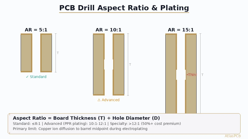
Aspect ratio impact: Press-fit holes in thick backplanes (3–6 mm) can have high aspect ratios (10:1+), making uniform plating challenging. Advanced plating processes (PPR - Periodic Pulse Reverse) are recommended for high-aspect-ratio press-fit holes. For more on aspect ratio considerations, see our [aspect ratio via design guide]/blog/pcb-aspect-ratio-via-design/).
Surface Finish in Press-Fit Holes
The surface finish inside the press-fit hole affects insertion force, retention force, and long-term reliability:
| Surface Finish | Suitability | Notes |
|---|---|---|
| Bare copper (with OSP) | Excellent | Most common for press-fit — consistent surface |
| ENIG | Good | Adds ~5 µm to hole diameter — account in sizing |
| Immersion Tin | Good | Smooth surface, be aware of tin whisker risk |
| HASL | Not Recommended | Uneven tin deposits change hole diameter unpredictably |
| Hard gold (electrolytic) | Excellent | Used for connector contact areas, expensive |
HASL warning: Hot Air Solder Leveling deposits tin unevenly inside through-holes, especially in high-aspect-ratio holes. This changes the effective hole diameter in an unpredictable manner and should be avoided for press-fit applications.
For complete surface finish comparison, see our [surface finish guide]/blog/pcb-surface-finish-guide/).
Hole Wall Quality
Beyond plating thickness and finish, the hole wall surface quality is critical:
- No copper nodules: Nodules create localized high-stress points during pin insertion
- No voids: Plating voids reduce contact area and create potential corrosion sites
- Minimal roughness: Surface roughness Ra should be <5 µm after plating
- Complete desmear: Residual resin smear on the hole wall prevents proper copper adhesion and creates weak spots
- No drill burrs: Entry and exit burrs must be completely removed
Board Design Considerations
Stackup and Thickness
Press-fit applications often involve thick, high-layer-count boards:
Backplane typical specifications:
- Layer count: 12–40+ layers
- Board thickness: 2.4–6.0 mm
- Copper weight: 1 oz (35 µm) signal, 2 oz (70 µm) power layers
- Material: Standard FR-4, high-Tg FR-4, or low-loss (for high-speed)
Thickness impact on press-fit:
- Thicker boards provide more barrel length for gas-tight contact
- Minimum engagement length: 1.0 mm of barrel contact recommended
- Aspect ratio of press-fit holes must be managed — use our [stackup calculator]/blog/pcb-stackup-calculator/) for planning
Thermal Pad and Anti-Pad Design
On inner copper layers, the press-fit hole has associated clearances:
- Connected layers: Thermal relief connections to inner planes (standard 4-spoke pattern)
- Non-connected layers: Anti-pad (clearance hole) in copper pours — minimum 0.25 mm clearance from hole edge to copper
- Power plane connections: Direct connection (no thermal relief) for minimum resistance on power pins
Back-Drilling Considerations
Many backplane designs combine press-fit connectors with high-speed signal routing, requiring back-drilling:
- Back-drilled holes and press-fit holes may be on the same connector
- Ensure back-drill does not interfere with press-fit engagement zone
- Back-drill stub length should still provide adequate barrel for press-fit contact
- Document which holes require back-drilling vs. which are press-fit in the fabrication drawing
For signal integrity in backplane applications, refer to our [signal integrity guide]/blog/signal-integrity-pcb-design-guide/).
IPC-9797 Compliance
Overview of IPC-9797
IPC-9797 “Press-Fit Standard for Automotive and Telecommunication Applications” defines:
- Design requirements — Hole sizing, plating, and PCB parameters
- Process requirements — Insertion speed, force monitoring, press equipment
- Qualification testing — A rigorous test program to validate the press-fit connection
Key IPC-9797 Requirements
Insertion Force:
- Maximum insertion force per pin must not exceed the connector manufacturer’s specification
- Typical: 30–80 N per pin for eye-of-needle designs
- Total insertion force for a multi-pin connector = per-pin force × number of pins
- The press equipment must be capable of the total force with adequate margin
Retention Force:
- After insertion, each pin must maintain a minimum retention (pull-out) force
- Typical requirement: ≥30 N per pin
- Tested by pulling individual pins from the board with a force gauge
- Retention force must be maintained after environmental testing (thermal cycling, humidity)
Gas-Tightness:
- The connection must be gas-tight per IPC-9797 criteria
- Measured by contact resistance: typically <5 mΩ initial, <10 mΩ after environmental stress
- Low and stable contact resistance indicates a gas-tight interface that prevents oxidation
Qualification Test Program
IPC-9797 qualification typically includes:
| Test | Condition | Pass Criteria |
|---|---|---|
| Insertion force | Monitor during insertion | Within manufacturer spec |
| Retention force | Pull-out test | ≥30 N (or per spec) |
| Contact resistance (initial) | 4-wire measurement | <5 mΩ |
| Thermal cycling | -40°C to +125°C, 1000 cycles | ΔR <5 mΩ |
| Humidity exposure | 85°C/85% RH, 1000 hours | ΔR <5 mΩ |
| Vibration | Per automotive spec (e.g., LV 214) | No change in resistance |
| Current cycling | Rated current, 1000 cycles | ΔR <5 mΩ |
| Mechanical shock | Per application spec | No pin displacement |
For comprehensive testing approaches, see our [PCB testing methods guide]/blog/pcb-testing-methods/).
Press-Fit Insertion Process
Equipment Requirements
Press equipment types:
- Pneumatic press: 1–50 kN capacity, suitable for small connectors
- Servo-electric press: 5–200 kN capacity, precise force/speed control, preferred for production
- Hydraulic press: 10–500 kN capacity, for very large connectors
Critical press parameters:
- Insertion speed: 0.5–5 mm/sec (too fast risks barrel damage; too slow reduces throughput)
- Force monitoring: Real-time force vs. displacement curve monitoring is essential
- Alignment: Press tool must maintain perpendicularity within ±0.1° to the board surface
- Support: The board must be supported close to the insertion point to prevent flexing
Force-Displacement Monitoring
The force vs. displacement curve during insertion is the primary quality indicator:
Typical curve characteristics:
- Initial contact: Force rises as pin enters the hole
- Compliance zone engagement: Force increases more steeply as the compliant section enters the barrel
- Peak insertion force: Maximum force occurs as the widest part of the compliant zone passes through the hole
- Seating: Force decreases and stabilizes as the pin reaches its final position
Abnormal curve indicators:
- Force too high: Hole too small, plating too thick, or barrel obstruction
- Force too low: Hole too large, insufficient plating, or pin damage
- Force spikes: Copper nodules, burrs, or plating defects in the hole
- No compliance zone: Pin not properly engaged — possible misalignment
Process Control
Insertion monitoring per IPC-9797:
- Monitor force vs. displacement for every pin (100% monitoring)
- Set upper and lower force limits (force window)
- Set displacement limits (pin must reach correct depth)
- Log all data for traceability
- Automatically flag out-of-specification insertions
Common Design Mistakes and Solutions
Mistake 1: Using Standard Via Tolerances
Problem: Specifying standard ±0.10 mm tolerance for press-fit holes Impact: 50% of holes may be too large or too small for reliable press-fit Solution: Specify ±0.05 mm tolerance as a separate drill class; communicate the press-fit requirement to your fabricator
Mistake 2: Insufficient Annular Ring
Problem: Using minimum annular ring from standard design rules Impact: Pad lift during press-fit insertion, especially on inner layers Solution: Increase annular ring to ≥0.25 mm for press-fit holes; use non-functional pads on inner layers to increase support
Mistake 3: HASL Surface Finish on Press-Fit Holes
Problem: HASL deposits tin unevenly in press-fit holes Impact: Unpredictable hole diameter changes; inconsistent insertion and retention forces Solution: Use bare copper with OSP, ENIG, or immersion tin for press-fit holes; if board also has SMT components requiring HASL, use selective surface finish
Mistake 4: No Fabrication Notes for Press-Fit
Problem: Press-fit holes not called out specifically in fabrication documentation Impact: Fabricator treats press-fit holes like standard vias — wider tolerance, less inspection Solution: Add specific notes: “Press-fit holes per IPC-9797. Finished hole diameter 1.02 ±0.05 mm. 100% hole diameter verification required.”
Mistake 5: Ignoring Board Flex During Insertion
Problem: No board support near insertion points Impact: Board flexes during insertion, causing internal barrel stress, pad lift, or cracking Solution: Design press tooling with board support within 15 mm of all press-fit holes; for large connector arrays, use progressive insertion (insert in sections)
Advanced Topics
High-Speed Press-Fit Connections
For press-fit connectors carrying high-speed signals (>10 Gbps):
- Impedance control through the press-fit hole is critical
- The press-fit hole acts as a via stub — back-drilling may be required
- Use press-fit connectors with controlled impedance pin designs
- Simulate the press-fit via discontinuity in your signal integrity model
- Consider TE Connectivity STRADA Whisper or Amphenol Xcede for >25 Gbps
Press-Fit in Flexible and Rigid-Flex PCBs
Press-fit in flex or rigid-flex boards requires special consideration:
- Only insert press-fit pins in rigid sections
- Minimum rigid section length: 3× board thickness around press-fit holes
- Additional support during insertion to prevent flex section damage
- Increased annular ring (≥0.30 mm) to compensate for reduced rigidity
Press-Fit Combined with Soldering
Some connectors combine press-fit pins (for power and ground) with soldered pins (for signal). Design considerations:
- Press-fit insertion must occur after soldering to avoid thermal damage to the press-fit connection
- Alternatively, use a connector designed for mixed attachment (press-fit pins in the same connector body as solder tails)
- Clearly identify which holes are press-fit vs. solder in your assembly documentation
For more on press-fit connector design considerations, see our dedicated [press-fit connector guide]/blog/press-fit-connector-pcb-design/).
Conclusion
Press-fit via design requires attention to detail beyond standard PCB through-hole design. The key specifications to remember:
- Hole diameter tolerance: ±0.05 mm (much tighter than standard PTH)
- Copper plating: ≥25 µm average, smooth, uniform, void-free
- Surface finish: Bare copper with OSP or ENIG preferred; avoid HASL
- Annular ring: ≥0.25 mm on all layers for insertion force resistance
- IPC-9797: The governing standard for qualification and production
- Force monitoring: 100% insertion force monitoring during production
- Fabrication communication: Press-fit holes must be clearly identified with separate drill class and tight tolerances
Successful press-fit implementation requires close collaboration between the PCB designer, connector manufacturer, fabricator, and assembly house. Atlas PCB provides specialized fabrication support for press-fit applications including tight-tolerance hole drilling, advanced plating processes, and 100% hole diameter verification.
Atlas PCB specializes in press-fit PCB fabrication with tight-tolerance drilling, advanced copper plating, and IPC-9797 compliant hole quality for automotive and telecom applications. Contact us for engineering support and a free DFM review on your next project.
Further Reading
- [Rogers PCB Fabrication: Material Sourcing, Lead Times & Quality Control]/blog/rogers-pcb-fabrication/)
- [PCB Manufacturer with Engineering Review: Why Human DFM Audit Matters]/blog/pcb-manufacturer-engineering-review/)
- [ENEPIG vs ENIG: Which PCB Surface Finish for Your Design?]/blog/enepig-vs-enig/)
- [PCB Surface Finish Selection — ENIG vs HASL vs OSP vs Hard Gold vs ENEPIG]/blog/pcb-surface-finish-enig-hasl-osp-hard-gold-enepig/)
- [BGA Pad Design and Via-in-Pad: How to Prevent Solder Voiding in High Pin-Count BGA Assemblies]/blog/bga-pad-design-via-in-pad-solder-voiding-prevention/)
- HDI PCB Manufacturing
About AtlasPCB — We specialize in complex PCB manufacturing for HDI, RF, and high-reliability applications. Explore our full PCB manufacturing capabilities . Every order includes free engineering review. Get your quote.
Reviewed by AtlasPCB Engineering Team — IPC-certified manufacturing specialists with 15+ years of production experience in HDI, RF, and high-reliability PCB fabrication. Content based on factory floor data and real customer design reviews.
- press-fit
- connector
- via-design
- ipc-9797
- backplane