· AtlasPCB Engineering · Engineering · 8 min read
Substrate Integrated Waveguide (SIW) PCB Design: Filters, Couplers and Antennas for mmWave Applications
Master SIW design on standard PCB substrates. Learn via fence rules, cutoff frequency calculations, transition design from microstrip to SIW, and practical fabrication guidelines for 24–77 GHz applications.
Introduction: Why Waveguides on a PCB?
As wireless systems push into the millimeter-wave spectrum — 24 GHz automotive radar, 28/39 GHz 5G, 60 GHz WiGig, and 77 GHz ADAS — traditional planar transmission lines like microstrip and stripline hit fundamental performance walls. Radiation loss increases with frequency squared, surface waves degrade isolation, and the unloaded Q-factor of microstrip resonators drops below 100 at 60 GHz.
Rectangular waveguides solve these problems beautifully — but they are bulky metallic structures impossible to integrate with planar circuits. Substrate Integrated Waveguide (SIW) bridges this gap by synthesizing a rectangular waveguide entirely within a printed circuit board using rows of plated through-holes as electric sidewalls.
This guide covers everything a hardware engineer needs to design, simulate, and manufacture SIW structures on standard PCB substrates — from fundamental mode analysis through practical fabrication rules that any competent PCB manufacturer can execute.
Fundamental SIW Theory
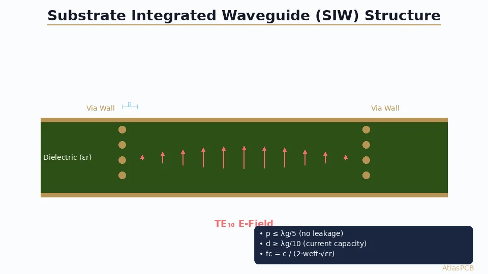
How SIW Works
A substrate integrated waveguide consists of:
- Top and bottom copper planes — acting as the broad walls of a rectangular waveguide
- Two rows of metallic vias — acting as the narrow sidewalls
- Dielectric substrate — filling the waveguide interior
The dominant propagation mode is TE₁₀, identical to a conventional rectangular waveguide. The key difference: the solid metallic sidewalls are replaced by a periodic via fence, which introduces small radiation leakage if not designed correctly.
Equivalent Width Calculation
The effective width of an SIW is slightly different from the physical via-center-to-via-center distance due to the gaps between vias. The standard empirical formula (Cassivi et al.) gives:
w_eff = w_siw - 1.08 × (d²/p) + 0.1 × (d²/w_siw)
Where:
- w_siw = center-to-center distance between via rows
- d = via diameter
- p = via pitch (center-to-center spacing along the row)
Cutoff Frequency
The TE₁₀ cutoff frequency is:
f_c = c / (2 × w_eff × √εr)
Where c is the speed of light and εr is the substrate dielectric constant. For single-mode operation, the operating frequency must be between f_c(TE₁₀) and f_c(TE₂₀) = 2 × f_c(TE₁₀).
Design Example: 77 GHz Automotive Radar
For a 77 GHz SIW on Rogers RO3003 (εr = 3.0, h = 0.127 mm):
- Target: TE₁₀ cutoff at ~55 GHz (operating band 76–81 GHz)
- w_eff = c / (2 × 55 GHz × √3.0) = 1.575 mm
- With d = 0.2 mm, p = 0.4 mm: w_siw ≈ 1.60 mm
- Via fence: 0.2 mm drill, 0.4 mm pitch, plated through
This is entirely achievable with standard PCB manufacturing — no exotic processes required.
Via Fence Design Rules
The via fence is the heart of SIW performance. Poorly designed vias leak radiation and destroy the waveguide’s advantage over microstrip.
Critical Parameters
| Parameter | Rule | Rationale |
|---|---|---|
| Via diameter (d) | d ≥ λg/10 | Adequate current-carrying capacity |
| Via pitch (p) | p ≤ 2d | Minimize slot radiation between vias |
| Pitch-to-wavelength | p ≤ λg/5 | Prevent bandgap effects |
| Via-to-edge clearance | ≥ 3d | Prevent drill breakout |
Radiation Leakage Budget
The leakage loss per unit length follows:
α_leak ∝ (p/d)² × exp(-π×d/p)
For p/d = 2.0 (the maximum recommended ratio), leakage loss is approximately 0.01 dB/λg — negligible compared to dielectric and conductor losses.
For tighter designs (p/d ≤ 1.5), leakage drops below 0.001 dB/λg, making it entirely insignificant.
Manufacturing Considerations
Standard PCB drill capabilities align well with SIW requirements:
- Mechanical drill: 0.15 mm minimum (perfect for SIW above 40 GHz)
- Laser drill: 0.075 mm minimum (enables SIW up to 110 GHz)
- Drill positional accuracy: ±0.025 mm (must be included in via fence tolerance budget)
- Plating: Standard electroless + electrolytic copper (20–25 μm wall thickness adequate)
Need SIW PCBs for mmWave Applications?
AtlasPCB manufactures precision RF boards with ±0.025 mm drill registration — critical for via fence performance at 77 GHz and above.
Request RF PCB Quote →Microstrip-to-SIW Transitions
Efficient coupling between standard microstrip feed lines and the SIW is essential. Several proven transition topologies exist:
Tapered Microstrip Transition
The most common approach: a microstrip line gradually widens into the SIW aperture over a quarter-guided-wavelength. The taper transforms the quasi-TEM microstrip mode into the TE₁₀ SIW mode.
Design procedure:
- Calculate 50 Ω microstrip width for your substrate
- Determine SIW aperture field distribution width
- Design linear or cosine taper over λg/4 length
- Typical return loss: > 15 dB over 15% bandwidth
Probe Coupling (Via Transition)
A single via connects microstrip to the SIW bottom plane, acting as a probe antenna exciting the TE₁₀ mode. Position the probe at w_siw/2 (center) and λg/4 from a short-circuit end.
Advantages: Compact, good for multilayer transitions between SIW on different layers. Limitations: Narrower bandwidth (~8–10%) without matching network.
Coplanar Waveguide (CPW) Transition
For wafer-probe measurement or CPW-based MMICs, a CPW-to-SIW transition using slot coupling provides wideband performance (>20% bandwidth) with return loss better than 20 dB.
SIW Component Design
Bandpass Filters
SIW cavity filters offer unloaded Q-factors of 300–500 at 60 GHz — 3–5× better than microstrip coupled-line filters. Common topologies:
Iris-coupled cavity filter:
- Inductive irises (narrowed via gaps) between λg/2 resonant cavities
- Bandwidth control via iris opening width
- 4th-order Chebyshev: typically 0.8–1.2 dB insertion loss at 60 GHz
Post-wall coupled filter:
- Internal via posts act as inductive coupling elements
- Easier to manufacture than iris (just additional vias)
- Excellent for 5–10% fractional bandwidth
Directional Couplers
SIW Riblet short-slot couplers provide 3 dB coupling with excellent phase balance:
- Two SIW channels share a common broad wall section
- Coupling controlled by shared-wall length
- Typical performance: ±0.3 dB amplitude, ±3° phase balance over 10% bandwidth
Slot Array Antennas
SIW provides an ideal feed structure for slot antenna arrays:
- Longitudinal slots cut in the top copper plane
- Slot spacing = λg for broadside radiation
- 16-element SIW slot array at 77 GHz: 18 dBi gain, 45% efficiency
- No external feed network needed — the SIW IS the feed
Material Selection for SIW
Key Material Parameters
| Material | εr | Df | Suitable Frequency | Cost Index |
|---|---|---|---|---|
| FR-4 (standard) | 4.3 | 0.020 | < 6 GHz | 1× |
| Rogers RO4003C | 3.38 | 0.0027 | < 40 GHz | 3× |
| Rogers RO3003 | 3.00 | 0.0013 | < 80 GHz | 5× |
| Isola Astra MT77 | 3.00 | 0.0017 | < 77 GHz | 4× |
| Rogers RT/duroid 5880 | 2.20 | 0.0009 | < 110 GHz | 8× |
| LCP (liquid crystal polymer) | 3.16 | 0.0025 | < 100 GHz | 6× |
Selection Guidelines
- 24 GHz (ISM, radar): RO4003C offers excellent cost-performance balance
- 28/39 GHz (5G FR2): RO3003 or Astra MT77 for base station antenna feed
- 60 GHz (WiGig, V-band): RO3003 minimum, RT/5880 preferred
- 77 GHz (automotive): RO3003 or LCP for volume production
Substrate Thickness Impact
Thinner substrates reduce conductor loss (less current spreading) but make transitions narrower-band. Typical choices:
- 0.127 mm (5 mil) — ideal for 60–77 GHz, tight coupling
- 0.254 mm (10 mil) — good for 24–40 GHz, easier fabrication
- 0.508 mm (20 mil) — suitable for sub-20 GHz SIW
Fabrication and Tolerance Guidelines
Critical Fabrication Specifications
For a reliable SIW PCB order, specify:
- Drill diameter tolerance: ±0.025 mm (critical for cutoff frequency)
- Drill position tolerance: ±0.025 mm (affects waveguide width uniformity)
- Copper plating thickness: ≥20 μm wall (adequate for skin depth at mmWave)
- Laminate thickness tolerance: ±10% (affects impedance and cutoff)
- Surface roughness: Rz ≤ 2 μm on inner surfaces (reduces conductor loss)
Common Manufacturing Issues
Problem: Via drill wander at high aspect ratios
- Solution: Use laser drilling for substrates < 0.2 mm thick
- Alternative: Reduce aspect ratio with controlled-depth drill from both sides
Problem: Copper surface roughness increasing loss
- Solution: Specify HVLP (Hyper Very Low Profile) copper foil
- Impact: 0.5–1.0 dB/cm reduction at 77 GHz vs standard ED foil
Problem: Registration between drill layers
- Solution: X-ray registration with fiducials on every panel
- Critical for multilayer SIW where via fences must align across layers
SIW vs. Competing Technologies
When to Use SIW
✅ Choose SIW when:
- Operating above 24 GHz where microstrip Q degrades
- Filter rejection > 40 dB required (SIW cavities provide steep skirts)
- High isolation between channels needed (e.g., diplexers, multiplexers)
- Antenna feed network must minimize loss
- Integration with planar circuits is essential
❌ Avoid SIW when:
- Operating below 10 GHz (SIW width becomes impractically large)
- Ultra-wideband operation needed (SIW is inherently band-limited: 2:1 bandwidth max)
- Lowest-cost consumer product where FR-4 microstrip suffices
- Rapid prototyping without mmWave simulation capability
SIW vs. Air-Filled Waveguide
| Parameter | SIW | Air-Filled WR-xx |
|---|---|---|
| Q-factor (60 GHz) | 300–500 | 2000–5000 |
| Size (footprint) | 1× (planar) | 5–10× |
| Integration | SMT compatible | Requires transitions |
| Cost (volume) | $5–15/board | $50–200/assembly |
| Manufacturing | Standard PCB | CNC machining |
For most commercial applications, SIW’s Q-factor is sufficient, and the integration and cost advantages are decisive.
Design Workflow: From Concept to Gerber
Step 1: System Specification
- Define operating frequency band and fractional bandwidth
- Specify insertion loss budget, rejection requirements
- Determine number of SIW components (filters, couplers, antennas)
Step 2: Material and Stackup Selection
- Choose laminate based on frequency and loss budget
- Define substrate thickness for optimal mode confinement
- Specify copper type (HVLP for mmWave)
Step 3: SIW Dimensioning
- Calculate effective width for target cutoff frequency
- Size via fence: diameter, pitch, clearance
- Verify single-mode operation bandwidth
Step 4: 3D EM Simulation
- Use HFSS, CST, or openEMS for full-wave analysis
- Model actual via geometry (barrel, pad, antipad)
- Include surface roughness model (Huray or Hammerstad)
- Optimize transitions for return loss > 15 dB
Step 5: Layout and DFM Review
- Generate drill files with tight tolerance callouts
- Verify via-to-via spacing meets manufacturer minimums
- Check copper balance for lamination flatness
- Include test coupons (thru-line, resonator, short)
Step 6: Manufacturing and Test
- First-article inspection of via position accuracy
- VNA measurement with probe station or connector launches
- Compare measured vs. simulated S-parameters
Advanced SIW Techniques
Half-Mode SIW (HMSIW)
By cutting an SIW along its longitudinal symmetry plane, you get half-mode SIW with:
- 50% width reduction (critical at low frequencies)
- Same propagation characteristics (magnetic wall boundary at cut)
- Slightly higher radiation from open edge
- Ideal for compact filters below 24 GHz
Folded SIW (FSIW)
A folded SIW stacks two half-height waveguides, reducing width by 50% while maintaining full-height performance. Requires multilayer PCB with:
- Three copper layers (top, middle, bottom)
- Via fences on both halves
- Slot coupling between layers
SIW with Embedded Components
Active devices (amplifiers, mixers, switches) can be embedded within SIW by:
- Creating local cavities for component placement
- Via-fence around component for isolation
- Probe transitions from SIW to component pads
Further Reading
For deeper dives into related RF PCB design topics:
- RF Via Stitching and Ground Plane Isolation
- mmWave PCB Material Selection: Rogers, Megtron, and LCP for 5G/6G
- High-Frequency PCB Substrate Selection: Dk and Df Guide
- RF Transmission Line Loss Budgeting for 5G mmWave PCB
Designing SIW structures for automotive radar, 5G infrastructure, or satellite communications? AtlasPCB provides precision RF PCB fabrication with the drill accuracy and plating uniformity that mmWave performance demands. Get a quote for your next RF project.
About AtlasPCB — We specialize in complex PCB manufacturing for HDI, RF, and high-reliability applications. Explore our RF and high-frequency PCB services . Every order includes free engineering review. Get your quote.
Reviewed by AtlasPCB Engineering Team — IPC-certified manufacturing specialists with 15+ years of production experience in HDI, RF, and high-reliability PCB fabrication. Content based on factory floor data and real customer design reviews.
- substrate integrated waveguide
- SIW
- mmWave PCB
- RF filter
- waveguide antenna
- 77 GHz radar
- 5G
- PCB design