· AtlasPCB Engineering · Engineering · 8 min read
RF Transmission Line Loss Budgeting: Calculating Insertion Loss for 5G mmWave PCBs
Master insertion loss budgeting for 5G mmWave PCB designs. Learn how conductor loss, dielectric loss, and radiation loss interact at 28–77 GHz, with practical stackup and material selection strategies.
Why Loss Budgeting Matters for 5G mmWave PCBs
The transition from sub-6 GHz to millimeter-wave (mmWave) frequencies in 5G NR has fundamentally changed how PCB designers approach signal path planning. At 28 GHz (n257/n258 bands) and 39 GHz (n260), every 0.1 dB of unexpected loss directly reduces link margin — potentially requiring larger antenna arrays or higher transmit power to compensate.
Loss budgeting is the systematic process of predicting, allocating, and managing insertion loss across every element in an RF signal path before committing to fabrication. Unlike lower-frequency designs where generous link margins mask material and routing inefficiencies, mmWave systems demand sub-decibel accuracy in loss prediction.
This guide breaks down the physics of each loss mechanism, provides closed-form equations suitable for spreadsheet-based budgeting, and maps material/process choices to measurable performance at frequencies from 24 GHz through 77 GHz.
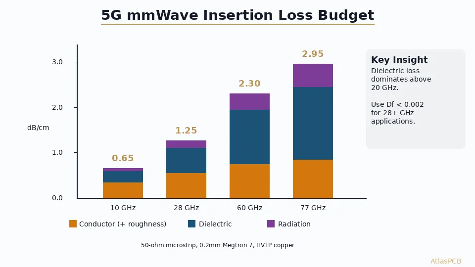
The Three Pillars of Transmission Line Loss
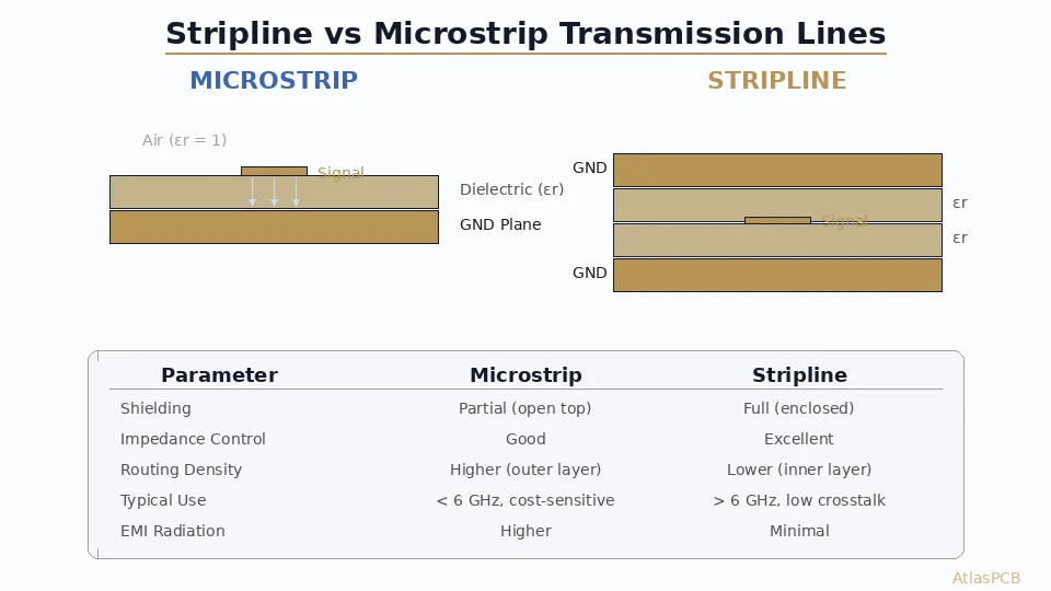
Every PCB transmission line — whether microstrip, stripline, coplanar waveguide (CPW), or substrate-integrated waveguide (SIW) — dissipates energy through three mechanisms:
1. Conductor Loss (α_c)
Conductor loss arises from the finite conductivity of copper traces and reference planes. At mmWave frequencies, skin depth shrinks to approximately 0.4 μm at 28 GHz and 0.26 μm at 60 GHz. This means current concentrates in an extremely thin surface layer, making copper surface roughness a dominant factor.
Key formula (Hammerstad-Jensen model):
α_c = Rs / (Z₀ × W_eff) [Np/m]Where Rs = √(π×f×μ₀/σ) is the surface resistance, Z₀ is characteristic impedance, and W_eff is the effective conductor width.
Surface roughness correction (Huray model):
The Huray snowball model provides the most accurate roughness correction for modern foil types:
K_rough = 1 + (2/π) × arctan(1.4 × (Δ/δ)²)Where Δ is RMS roughness and δ is skin depth. For standard ED copper (Rz ≈ 5 μm), this adds 40–80% additional loss at 60 GHz compared to smooth copper. RTF (Reversed Treated Foil, Rz ≈ 1.5 μm) or HVLP (Rz < 1 μm) foils reduce this penalty to 10–20%.
2. Dielectric Loss (α_d)
Dielectric loss results from molecular polarization lag in the substrate material as the electromagnetic field oscillates. It scales linearly with frequency:
α_d = (π × f × √ε_eff × tan δ) / c [Np/m]This linear frequency dependence means that dielectric loss becomes the primary bottleneck above 20 GHz. A material with Df = 0.004 (like standard FR-4) generates 4× more dielectric loss than one with Df = 0.001 (like Rogers RO3003) at any given frequency.
Material classes for mmWave:
| Material Category | Df @ 10 GHz | Relative Cost | Typical Use |
|---|---|---|---|
| Standard FR-4 | 0.018–0.022 | 1× | < 3 GHz only |
| Low-loss FR-4 (Megtron 4) | 0.005–0.007 | 2.5× | Sub-6 GHz 5G |
| Very-low-loss (Megtron 7) | 0.001–0.002 | 4× | 24–40 GHz |
| PTFE/Ceramic (Rogers 3003) | 0.001 | 6× | 40–77 GHz |
| Ultra-low-loss PTFE (TLY-5) | 0.0009 | 8× | 60+ GHz, radar |
3. Radiation and Leakage Loss (α_r)
At mmWave frequencies, transmission line discontinuities become electrically significant. Bends, width transitions, and gaps can radiate energy into substrate modes or free space. Substrate-mode excitation is particularly problematic when substrate thickness exceeds λ/4 in the dielectric.
Critical thickness constraint:
h_max < c / (4 × f × √(ε_r - 1))For Rogers RO4003C (εr = 3.55) at 60 GHz: h_max < 0.66 mm. Substrates thicker than this support surface waves that leak energy along the board edge.
Building Your Loss Budget Spreadsheet
A practical loss budget breaks the signal path into segments and sums contributions:
Step 1: Define the Signal Path
Map every element from RFIC pad to antenna feed:
- Wire bond / flip-chip transition
- Package substrate trace
- BGA-to-board transition
- Board-level transmission line (main routing)
- Via transitions (layer changes)
- Connector interfaces (if applicable)
- Antenna feed network
Step 2: Calculate Per-Segment Loss
For each straight transmission line segment:
Total_loss_segment = (α_c × K_rough + α_d + α_r) × LengthFor each discontinuity, use measured S-parameter data or full-wave simulation results. Typical values:
| Discontinuity | Loss @ 28 GHz | Loss @ 60 GHz |
|---|---|---|
| Microstrip 90° bend (mitered) | 0.05–0.1 dB | 0.1–0.2 dB |
| Microstrip-to-stripline via | 0.2–0.4 dB | 0.4–0.8 dB |
| CPW-to-microstrip transition | 0.1–0.2 dB | 0.2–0.5 dB |
| SMA connector (end-launch) | 0.15 dB | 0.3–0.5 dB |
| BGA ball (signal) | 0.1–0.2 dB | 0.2–0.4 dB |
Step 3: Add Margin
Production variation, temperature effects, and aging add uncertainty. Standard practice allocates:
- ±10% for material Df variation (lot-to-lot)
- ±15% for etching tolerance impact on Z₀
- 0.5–1.0 dB fixed margin for unexpected coupling/resonances
- Temperature coefficient: +0.01 dB/°C/GHz for most PTFE materials
ATLAS PCB — RF & MICROWAVE SPECIALISTS
Need a mmWave PCB with Guaranteed Insertion Loss?
We manufacture Rogers, Taconic, and hybrid RF stackups with TRL-calibrated VNA verification up to 67 GHz. Get your loss budget validated before production.
Request RF PCB Quote →Material Selection Strategy by Frequency Band
24–30 GHz (5G FR2 Band n257/n258)
At 28 GHz, both conductor and dielectric losses are significant. The optimal approach balances cost against performance:
Budget approach: For paths < 30 mm, Megtron 6 or Megtron 7 with HVLP foil often meets link budget requirements. For longer feeds (> 50 mm) or multi-channel systems with tight power budgets, Rogers RO4835 or RO3003 becomes necessary.
Typical loss budget (50 mm microstrip, Z₀ = 50Ω):
- Megtron 7 + HVLP foil: ~1.8 dB total
- Rogers RO4003C + RTF foil: ~1.4 dB total
- Rogers RO3003 + RA copper: ~0.9 dB total
37–43.5 GHz (5G FR2 Band n260)
At 39 GHz, dielectric loss dominates heavily. Standard low-loss materials hit diminishing returns; only ultra-low Df materials remain viable for paths > 20 mm.
57–71 GHz (WiGig / 802.11ad/ay)
The 60 GHz band demands the most aggressive material and geometry choices:
- Substrate thickness ≤ 0.254 mm (10 mil) to suppress surface waves
- PTFE or LCP substrates (Df < 0.002 mandatory)
- HVLP or rolled-annealed copper (Rz < 1.0 μm)
- Grounded coplanar waveguide (GCPW) preferred over microstrip
76–81 GHz (Automotive Radar)
Automotive radar operates at the highest commercial mmWave frequencies. Loss budgets are extremely tight because antenna gain must compensate for atmospheric absorption and target RCS variations:
- Typical path loss budget: < 2 dB for entire feed network
- Preferred materials: Rogers RO3003, Taconic TLY-5, AGC Meteorwave
- GCPW or SIW routing mandatory
- Substrate thickness: 0.127–0.254 mm
Copper Foil Selection and Roughness Impact
The single most underestimated variable in mmWave loss budgets is copper roughness. Production copper foils range from:
- Standard ED (electrodeposited): Rz = 4–7 μm — suitable only below 6 GHz
- RTF (Reverse Treated Foil): Rz = 1.5–3 μm — acceptable to 28 GHz
- HVLP (Hyper Very Low Profile): Rz = 0.8–1.5 μm — recommended for 28–60 GHz
- Rolled Annealed (RA): Rz = 0.3–0.5 μm — optimal above 40 GHz
Practical impact at 60 GHz (50Ω microstrip, 0.127 mm RO3003):
- With standard ED foil: α_c = 0.45 dB/cm
- With RTF foil: α_c = 0.28 dB/cm (38% reduction)
- With HVLP foil: α_c = 0.22 dB/cm (51% reduction)
This difference compounds over routing length. A 40 mm feed network saves 0.92 dB by switching from ED to HVLP — potentially eliminating the need for an additional LNA stage.
Via Transition Design for Minimal Loss
Layer transitions are necessary in complex mmWave boards but introduce significant loss if poorly designed. Key strategies:
Back-drilled Vias
Stub length resonance occurs when via stubs approach λ/4 at the operating frequency. At 28 GHz, a 1 mm stub creates a resonant null. Back-drilling removes the stub to within 0.1–0.2 mm of the signal layer, reducing transition loss from 0.8 dB to 0.2–0.3 dB.
Coaxial Via Structures
Surrounding a signal via with a ring of ground vias creates a coaxial-like structure that maintains impedance control through the transition. Optimal ground via spacing: < λ/8 at the operating frequency (< 0.67 mm at 60 GHz).
Via-in-Pad with Copper Fill
For flip-chip or wafer-level packages, via-in-pad with IPC-4761 Type VII fill provides the shortest, lowest-inductance path to internal routing layers.
Practical Loss Budget Example: 28 GHz 5G FEM
Consider a 5G Front-End Module on a 4-layer Rogers RO4835/RO4450F hybrid stackup:
Signal path: RFIC (QFN) → 15 mm microstrip L1 → via to L3 stripline → 25 mm stripline → via to L1 → 10 mm microstrip → antenna feed
| Segment | Length | Loss/Unit | Subtotal |
|---|---|---|---|
| QFN pad-to-trace | — | 0.15 dB | 0.15 dB |
| L1 microstrip (RO4835) | 15 mm | 0.12 dB/mm | 1.80 dB |
| Via L1→L3 (back-drilled) | — | 0.25 dB | 0.25 dB |
| L3 stripline (RO4450F) | 25 mm | 0.08 dB/mm | 2.00 dB |
| Via L3→L1 (back-drilled) | — | 0.25 dB | 0.25 dB |
| L1 microstrip (RO4835) | 10 mm | 0.12 dB/mm | 1.20 dB |
| Total predicted loss | 5.65 dB | ||
| Margin (+15%) | 0.85 dB | ||
| Budget total | 6.50 dB |
If the system link budget only allows 4 dB of board loss, this design needs revision — either shorter paths, better materials (RO3003 would save ~2.5 dB), or a different layer transition strategy.
Design Rules for Minimizing mmWave Loss
Based on production experience across hundreds of 5G and radar boards:
- Keep traces short — every millimeter counts above 28 GHz. Collocate RF components.
- Match foil to frequency — don’t use ED copper above 10 GHz, RTF above 40 GHz.
- Mind the surface finish — ENIG adds 0.05–0.15 dB/cm vs bare copper at 60 GHz. Immersion silver or OSP preferred for RF paths.
- Control substrate thickness — thinner is better for mode suppression (0.127–0.254 mm for signal layers above 40 GHz).
- Back-drill all through-vias in mmWave signal paths.
- Use ground coplanarity — add coplanar ground strips adjacent to microstrip for improved field confinement.
- Simulate discontinuities — budget values are estimates; final via/transition geometries need full-wave verification (HFSS, CST).
Measurement Verification: TRL Calibration
Once boards are fabricated, validating the loss budget requires accurate measurements. Thru-Reflect-Line (TRL) calibration using on-board standards provides the best accuracy for de-embedding fixture effects:
- Design TRL standards on the same panel as the product
- Minimum 3 line lengths for broadband calibration
- Account for reference plane shift in budget comparison
- Expect ±0.05 dB measurement uncertainty up to 40 GHz, ±0.1 dB to 67 GHz
Further Reading
- [RF & Microwave PCB Design: Materials, Stackup, and Manufacturing Guide]/blog/rf-microwave-pcb-design/)
- [PCB Via Transitions for RF Design: Coaxial, GCPW, and Antipad Optimization]/blog/pcb-via-transitions-rf-design-coaxial-gcpw-antipad/)
- [Rogers vs PTFE Material Selection for 5G RF PCBs]/blog/rf-pcb-rogers-vs-ptfe-material-selection-5g/)
- [Controlled Impedance PCB Design: Stackup Calculations and Manufacturing]/blog/controlled-impedance-pcb-design-stackup-calculations/)
Need help with your mmWave loss budget? AtlasPCB’s RF engineering team provides complimentary design reviews for complex 5G and radar PCB stackups. Get a free consultation →
About AtlasPCB — We specialize in complex PCB manufacturing for HDI, RF, and high-reliability applications. Explore our RF and high-frequency PCB services, or get an impedance-controlled PCB manufacturing . Every order includes free engineering review. Get your quote.
Reviewed by AtlasPCB Engineering Team — IPC-certified manufacturing specialists with 15+ years of production experience in HDI, RF, and high-reliability PCB fabrication. Content based on factory floor data and real customer design reviews.
- rf pcb
- 5g mmwave
- insertion loss
- transmission line
- dielectric loss
- conductor loss
- signal integrity
- rogers
- high frequency