· AtlasPCB Engineering · Engineering · 8 min read
How to Specify Via-in-Pad on Your PCB Fab Drawing: VIPPO Requirements, IPC-4761, and DFM Checklist
Complete guide to specifying via-in-pad plated over (VIPPO) on your fabrication drawing. Covers IPC-4761 fill types, dimensional requirements, common DFM errors, and the exact notes your fab drawing needs for reliable via-in-pad production.
Quick Answer: The Minimum Fab Drawing Callout
Your fabrication drawing must include this note (or equivalent) for any via-in-pad design:
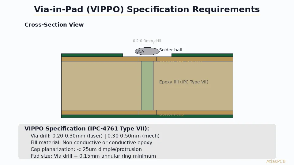
NOTE X: VIA-IN-PAD REQUIREMENT
All vias located within component pads (as identified on the fab drawing detail)
shall be filled and planarized per IPC-4761 Type VII.
- Fill material: Non-conductive epoxy (or conductive, specify if required)
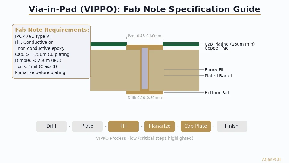
- Planarization: < 25um dimple, < 25um protrusion per IPC-4761
- Cap plating: Minimum 15um copper over filled via
- Via drill: [specify your drill diameter]
- Applicable pads: [list reference designators or pad sizes]Without this explicit callout, manufacturers may default to via tenting or partial fill — both of which cause assembly defects on fine-pitch BGAs.
Why Via-in-Pad Exists: The BGA Routing Problem
The proliferation of fine-pitch BGAs (0.4-0.65mm pitch) in modern electronics has created a routing density problem that via-in-pad solves elegantly. On a 0.5mm pitch BGA with a full array, the available routing channel between adjacent pads is approximately 0.15-0.20mm — far too narrow for a via and route-out on the same layer. The traditional “dog-bone” fanout pattern, where a short trace connects the BGA pad to a via placed outside the pad array, simply does not fit once pitch drops below 0.65mm for multi-row arrays.
Via-in-pad eliminates this constraint by placing the via directly within the component pad itself. The signal or power connection drops straight through the pad to an inner layer, freeing the surface routing channels entirely. For a 400-ball BGA on 0.5mm pitch, this can reduce the required routing layers from six to four — a significant cost and reliability improvement.
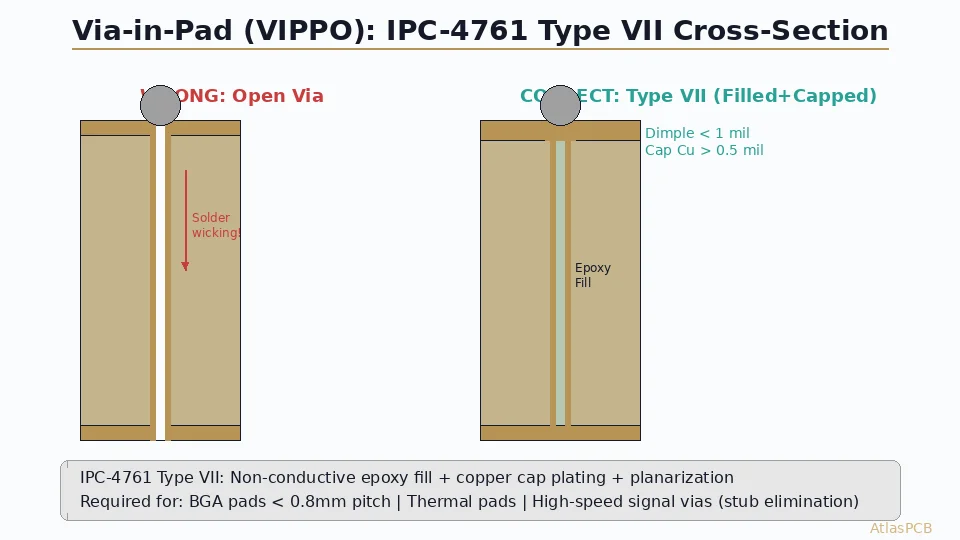
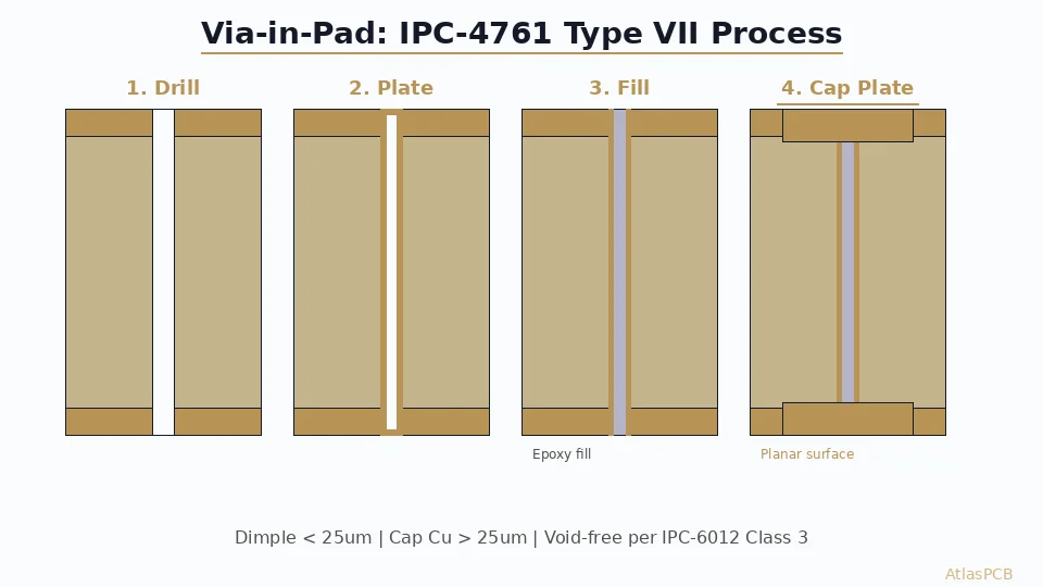
The challenge is that an unfilled via in a component pad creates serious assembly defects. During reflow soldering, solder wicks down into the open via barrel by capillary action, starving the joint above and creating voids. In our SMT assembly analysis, unfilled vias under BGA pads consistently produce 15-40% solder volume loss and void content exceeding 25% — well beyond the IPC-7095 acceptance criteria of 25% maximum voiding for Class 2 product. The VIPPO process (fill the via with epoxy, planarize, then plate over with copper) creates a flat, solderable surface that behaves identically to a solid pad.
HDI + VIA-IN-PAD CAPABILITY
Complex BGA Fanout Designs with Via-in-Pad
Laser and mechanical via-in-pad with IPC-4761 Type VII fill. Planarization to within 15um. Up to 5+N+5 HDI buildup with stacked microvias.
Upload Your BGA Design ›IPC-4761 Fill Types: Choosing the Right One
IPC-4761 defines seven via protection types, and engineers frequently confuse them. Only Types V and VII are appropriate for via-in-pad applications:
| IPC-4761 Type | Description | Via-in-Pad? | Typical Use |
|---|---|---|---|
| Type I | Tented (mask one side) | No | Standard vias, mask coverage |
| Type II | Tented (mask both sides) | No | Standard vias, both sides covered |
| Type III | Plugged (mask fill one side) | No | Prevent solder theft only |
| Type IV | Plugged (mask fill both sides) | No | Prevent solder theft both sides |
| Type V | Filled (non-conductive epoxy) | Partial | Via-in-pad where no pad above |
| Type VI | Filled and capped (one side) | Sometimes | Via-in-pad, one-sided assembly |
| Type VII | Filled and capped (both sides) | Yes | Full via-in-pad (VIPPO) |
For any design where a BGA or QFN thermal pad sits directly over a via, Type VII is the correct specification. Type V (filled but not capped) is acceptable only when the via is within a thermal pad that will have sufficient solder paste coverage to tolerate the slight surface irregularity of uncapped fill material.
The fill material choice matters for electrical performance. Non-conductive epoxy fill is standard and costs less — it works for signal vias and most power vias where the current path is through the copper barrel plating, not through the fill. Conductive epoxy fill (silver-loaded) or copper-filled vias provide 2-5x lower thermal resistance through the via, which matters only for thermal vias under power devices dissipating more than 2-3W. In our experience across thousands of via-in-pad designs, 95% of applications are well-served by standard non-conductive fill.
Common DFM Errors We Catch in Review
Our DFM engineering team reviews 200+ via-in-pad designs monthly. These are the five most common errors that cause manufacturing problems or assembly defects:
Error 1: Via drill too large for the pad. A 0.3mm mechanically drilled via in a 0.45mm pad leaves only 0.075mm annular ring per side — below the IPC Class 2 minimum of 0.05mm after registration tolerance is consumed. The fill process also becomes unreliable above 0.35mm drill diameter for single-pass dispense fill. Our recommendation: keep drill diameter below 65% of finished pad diameter for mechanically drilled via-in-pad.
Error 2: Missing fill callout. We estimate 30% of BGA designs arriving for quote have vias clearly placed within pads but no IPC-4761 callout on the fab drawing. Without the callout, our default process is via tenting — which will cause assembly voids on every ball over a via. We flag this in DFM review, but if you skip to production without review, you will get tented vias and an assembly problem.
Error 3: Via-in-pad on thermal pad without adequate via count. Engineers place one or two 0.3mm filled vias in a 3x3mm QFN thermal pad and expect meaningful heat transfer. The effective thermal conductivity of two filled vias across a 1.6mm board is approximately 0.5 W/mK of the available pad area — barely better than bare FR-4. For QFN thermal pads, we recommend a minimum via array density of 1.0mm pitch (giving 9 vias in a 3x3mm pad) with copper-filled vias for any component dissipating more than 1W.
Error 4: Mixing filled and unfilled vias in the same drill size. When your design has some 0.3mm vias as via-in-pad (requiring fill) and other 0.3mm vias as standard through-holes (no fill needed), you must differentiate them on the drill chart. Use different drill symbols or a dedicated fill designation layer. Otherwise, the manufacturer either fills all 0.3mm vias (adding cost) or fills none (causing assembly defects).
Error 5: Not accounting for cap plating in copper thickness. The cap plating process adds 15-25um of copper to the pad surface layer everywhere — not just over the filled vias. If your design requires tight impedance control on surface traces (which are now 15-25um thicker than expected), the impedance calculation must account for the additional copper. Call out your finished copper thickness requirement on the impedance table, and let the manufacturer adjust starting foil weight accordingly.
DFM REVIEW INCLUDED
Catch Via-in-Pad Errors Before They Cost You a Respin
Every order includes DFM review by our process engineering team. We flag annular ring violations, missing fill callouts, and thermal via density issues before production.
Submit for DFM Review ›Dimensional Requirements by Application
The required via-in-pad specifications vary by the component pitch and assembly process. Here is our recommended parameter set based on actual production results across IPC Class 2 and Class 3 assemblies:
| BGA Pitch | Max Via Drill | Min Pad Diameter | Min Annular Ring | Cap Flatness |
|---|---|---|---|---|
| 1.0mm | 0.40mm | 0.60mm | 0.10mm | 50um |
| 0.8mm | 0.35mm | 0.50mm | 0.075mm | 35um |
| 0.65mm | 0.30mm | 0.45mm | 0.075mm | 25um |
| 0.5mm | 0.25mm (laser preferred) | 0.35mm | 0.05mm | 25um |
| 0.4mm | 0.15mm (laser required) | 0.28mm | 0.05mm | 15um |
For pitches below 0.5mm, laser-drilled microvias are strongly preferred over mechanical drills. Laser vias at 0.10-0.15mm diameter produce cleaner fill results (fewer voids in the epoxy plug) and tighter cap planarization because the smaller void volume requires less fill material and shrinks less during cure. In our HDI production line, laser-drilled via-in-pad consistently achieves less than 10um cap deviation, versus 15-25um typical for mechanically drilled 0.25-0.35mm vias.
Complete Fab Drawing Template
Based on the most common via-in-pad configurations we produce, here is a complete fab drawing note template that covers all necessary parameters. Adapt the specific values to your design:
FABRICATION NOTES - VIA-IN-PAD REQUIREMENTS

1. All vias within component pads identified by drill symbol [X] on drill
   drawing shall be processed per IPC-4761 Type VII (filled and cap plated).

2. Fill material: Non-conductive epoxy per IPC-4761, cured per manufacturer
   specification.

3. Planarization requirement: Maximum 25um dimple (concavity) or 25um
   protrusion (convexity) measured from the surrounding copper surface.

4. Cap plating: Minimum 15um electrolytic copper over filled and planarized
   via. Cap plating shall blend smoothly with surrounding pad copper.

5. Via-in-pad drill sizes:
   - Symbol [X]: 0.25mm finished hole (for U1, U3, U7 BGA fanout)
   - Symbol [Y]: 0.30mm finished hole (for U2, U4 QFN thermal pads)

6. Via-in-pad vias shall NOT be visible in final pad surface after cap plating
   and surface finish application.

7. Inspection: 100% visual inspection of via-in-pad planarization per
   IPC-6012 Class [2/3] requirements. Cross-section sampling per lot.
ATLASPCB
Ready to Order Your Via-in-Pad Design?
Upload your Gerber files with the fab notes above. Our DFM team validates fill and cap parameters against your BGA specifications before production begins.
Get Instant Quote ›Reviewed by AtlasPCB Engineering Team — 15+ years in advanced PCB fabrication for RF, HDI, and rigid-flex applications.
Related Reading:
About AtlasPCB — We specialize in complex PCB manufacturing for HDI, RF, and high-reliability applications. Explore our HDI PCB manufacturing capabilities, or get an free engineering DFM review . Every order includes free engineering review. Get your quote.
Reviewed by AtlasPCB Engineering Team — IPC-certified manufacturing specialists with 15+ years of production experience in HDI, RF, and high-reliability PCB fabrication. Content based on factory floor data and real customer design reviews.
- via-in-pad
- VIPPO
- DFM
- PCB fab drawing
- BGA fanout