· Engineering · 6 min read
How to Specify Via-in-Pad for BGA Fanout: DFM Requirements and Fab Drawing Checklist
Complete DFM guide for specifying via-in-pad (VIPPO) on your PCB fab drawing. Covers hole sizes, plating fill requirements, cap plating thickness, IPC-4761 types, and the exact callouts your fabricator needs to build it right the first time.
Quick Answer: Via-in-Pad Fab Drawing Callout
Your fab drawing note should include all of these for via-in-pad pads:
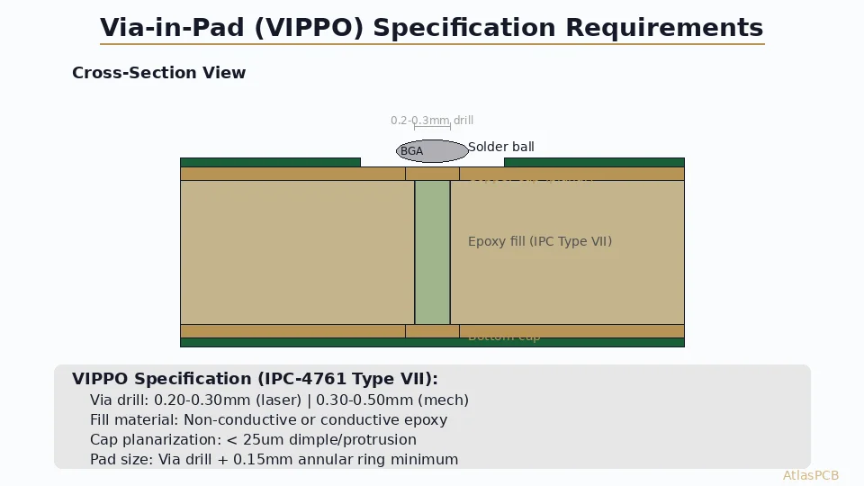
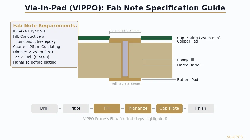
VIA-IN-PAD REQUIREMENTS (IPC-4761 Type VII):
- Via fill: Non-conductive epoxy per IPC-4761 Type VII
- Cap plating: Min 0.5 mil (12.7 μm) copper over fill
- Surface dimple: Max 1.0 mil (25 μm) concavity or convexity
- Surface finish applied over cap plating
- Via drill: [specify diameter] mm
- Applicable pads: [list reference designators or note "all BGA pads"]
If your fabricator asks “do you want filled vias?” — this is what they need from you.
Why Via-in-Pad Matters for BGA Routing
Standard dog-bone fanout (via adjacent to pad) works for BGAs down to 0.8mm pitch. Below that, there is no physical room for a via plus trace between adjacent pads.
Via-in-pad places the via directly inside the BGA pad, eliminating the dog-bone stub and giving you:
- Direct vertical connection from BGA ball to inner layer
- No via stub resonance (critical above 10 GHz)
- Shorter current path for power/ground
- Denser routing capability for 0.4-0.65mm pitch BGAs
The trade-off: your fabricator needs explicit DFM specs or they may process the vias incorrectly, leading to solder voiding, pad cratering, or assembly defects.
DFM REVIEW INCLUDED
We Check Your Via-in-Pad Specs Before Fabrication
AtlasPCB engineers review BGA pad definitions, via sizes, and fill requirements as part of every HDI order to prevent assembly issues.
Upload Gerber ›Complete DFM Parameter Table
| Parameter | Standard Requirement | High-Reliability Requirement |
|---|---|---|
| Fill material | Non-conductive epoxy | Per IPC-4761 Type VII |
| Cap plating Cu thickness | Min 0.5 mil (12.7 μm) | Min 0.8 mil (20 μm) |
| Max dimple (concavity) | 1.0 mil (25 μm) | 0.5 mil (12.7 μm) |
| Max protrusion (convexity) | 1.0 mil (25 μm) | 0.5 mil (12.7 μm) |
| Via drill (microvia) | 0.075-0.15 mm | 0.1 mm typical |
| Via drill (mechanical) | 0.2-0.3 mm | 0.2-0.25 mm |
| Aspect ratio limit | 0.8:1 (laser), 8:1 (mech.) | 0.6:1 (laser), 6:1 (mech.) |
| Pad diameter over via | Via + 6 mil min annular ring | Via + 8 mil min |
| Surface finish over cap | Any (ENIG, ImAg, OSP) | ENIG recommended |
Step-by-Step: How to Specify Via-in-Pad in Your Design
Step 1: Identify Which Pads Need Via-in-Pad
Not every via needs filling. Focus on:
- BGA pads where pitch prevents dog-bone routing (less than 0.8mm)
- Thermal pads (exposed pads) on QFN/DFN packages
- High-speed signal vias where stub resonance must be eliminated
- Power vias under large ICs where thermal resistance must be minimized
Step 2: Choose Via Size Based on Pitch
| BGA Pitch | Pad Diameter | Max Via Drill | Via Type |
|---|---|---|---|
| 1.0 mm | 0.5 mm | 0.3 mm | Mechanical |
| 0.8 mm | 0.4 mm | 0.25 mm | Mechanical |
| 0.65 mm | 0.35 mm | 0.2 mm | Mechanical |
| 0.5 mm | 0.25 mm | 0.15 mm | Laser microvia |
| 0.4 mm | 0.2 mm | 0.1 mm | Laser microvia |
Step 3: Specify in Your Fab Drawing
Include these exact notes on your fabrication drawing (Layer 0 or dedicated fab notes layer):
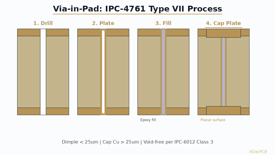
Note 1 — Via Fill Requirement:
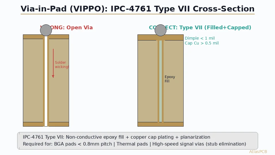
“All vias located within SMD pads (via-in-pad) shall be filled with non-conductive epoxy and planarized per IPC-4761 Type VII. Maximum surface dimple shall not exceed 25 micrometers (1.0 mil) concavity or convexity after cap plating.”
Note 2 — Cap Plating:
“Minimum 12.7 micrometers (0.5 mil) copper cap plating required over filled vias before surface finish application.”
Note 3 — Via Identification:
“Via-in-pad locations identified by [choose one]: all vias within SMD pad boundaries / drill chart callout / fab drawing detail view.”
Step 4: Verify Your Stackup Supports It
Common mistakes:
- Via drill too large for pad (annular ring violation after registration)
- Aspect ratio exceeding fab capability (0.3mm drill through 3.2mm board = 10.6:1)
- Forgetting that cap plating adds copper thickness to pad (affects solder paste volume)
HDI CAPABILITY
Laser Drill Down to 0.075mm
AtlasPCB supports via-in-pad with both laser microvias and mechanical drills. Up to 5+N+5 HDI buildup with stacked and staggered configurations.
View HDI Services ›Common DFM Mistakes to Avoid
Mistake 1: Not specifying dimple tolerance
Problem: Your fabricator fills vias but doesn’t planarize sufficiently. Result: 3-4 mil dimple causes solder paste print defects and BGA voiding above 25%.
Fix: Always specify maximum dimple in your fab notes. Standard: 1 mil. High-reliability: 0.5 mil.
Mistake 2: Via too close to pad edge
Problem: Registration tolerance causes via to break out of pad boundary. Exposed copper fill has no solderable surface finish.
Fix: Ensure minimum 3 mil (75 μm) annular ring from via edge to pad edge, accounting for drill registration tolerance (typically +/- 2 mil for mechanical, +/- 1 mil for laser).
Mistake 3: Forgetting thermal relief on power planes
Problem: Via-in-pad on power pins connected with full copper pour. During reflow, massive thermal mass prevents proper solder melting on that pad.
Fix: Use thermal relief on internal power connections for via-in-pad BGA pads, or discuss with your assembly house for adjusted reflow profiles.
Mistake 4: Specifying conductive fill without thermal need
Problem: Conductive epoxy fill costs 2-3x more than non-conductive fill and has no benefit for signal vias.
Fix: Use non-conductive fill for signal and I/O vias. Reserve conductive fill only for thermal vias under power components where thermal conductivity through the via is critical.
AVOID COSTLY RESPINS
Submit Your Design for DFM Check
We flag via-in-pad issues, annular ring violations, and aspect ratio problems before fabrication starts.
Get DFM Feedback ›IPC-4761 Via Protection Types Reference
| Type | Description | Use Case |
|---|---|---|
| I | Tented (covered with dry film) | Non-critical vias |
| II | Tented and covered (soldermask both sides) | Standard through-hole |
| III | Plugged (non-conductive paste, not planarized) | General SMD proximity |
| IV | Plugged and covered | Better plug, still not flat |
| V | Filled (conductive or non-conductive, planarized) | Thermal vias |
| VI | Filled and covered | Enhanced fill protection |
| VII | Filled and capped (planarized + copper cap) | Via-in-pad (VIPPO) |
Type VII is what you need for via-in-pad. Anything less risks assembly defects under BGA pads.
ATLASPCB
Ready to Order HDI Boards with Via-in-Pad?
Upload your Gerber files. We verify via-in-pad specs, stackup feasibility, and provide DFM feedback within 24 hours.
Get Instant Quote ›Related Reading:
About AtlasPCB — We specialize in complex PCB manufacturing for HDI, RF, and high-reliability applications. Explore our HDI PCB manufacturing capabilities, or get an free engineering DFM review . Every order includes free engineering review. Get your quote.
Reviewed by AtlasPCB Engineering Team — IPC-certified manufacturing specialists with 15+ years of production experience in HDI, RF, and high-reliability PCB fabrication. Content based on factory floor data and real customer design reviews.
- via-in-pad
- DFM
- BGA fanout
- PCB fabrication
- VIPPO