· AtlasPCB Engineering · Engineering · 11 min read
BGA Pad Design and Via-in-Pad: How to Prevent Solder Voiding in High Pin-Count BGA Assemblies
Master BGA pad design with via-in-pad plating techniques. Learn NSMD vs SMD pad strategies, via fill requirements, IPC-7095 compliance, and proven methods to achieve less than 25% voiding under 0.4mm-pitch BGAs.

Introduction: The BGA Voiding Problem
Ball Grid Array packages dominate modern electronics—from processors and FPGAs running data centers to RF transceivers in 5G base stations. As BGA pitch shrinks from 1.0 mm to 0.4 mm and below, the interaction between pad design, via placement, and solder joint formation becomes the critical factor determining assembly yield and long-term reliability.
Solder voiding—gas pockets trapped within the solder joint during reflow—is the most common defect in BGA assembly. A void larger than 25% of the pad area reduces thermal conductivity by the same proportion, increases current density in power connections, and creates stress concentration points that initiate fatigue cracks under thermal cycling.
The challenge intensifies with high pin-count BGAs (1000+ balls) where routing demands force vias directly under BGA pads. This via-in-pad approach is essential for fanout routing but introduces outgassing pathways that create voids unless properly managed.
This guide provides complete design rules for BGA pad design with via-in-pad, covering the IPC specifications, proven fill techniques, manufacturing process controls, and inspection criteria that separate reliable production from yield-killing defects. For related reading on copper plating processes that make via-in-pad possible, see our [electroless vs electrolytic copper plating guide]/blog/pcb-copper-plating-electroless-vs-electrolytic-hdi-vias/). Understanding [PCB surface finish options]/blog/pcb-surface-finish-osp-hasl-enig-immersion-silver-comparison/) is also essential for BGA pad design.
Understanding Void Formation Mechanisms
Why Voids Form Under BGA Balls
During reflow soldering, voids form through three primary mechanisms:
1. Via Outgassing (Most Common with Via-in-Pad)
Even “filled” vias can contain entrapped moisture, flux volatiles, or air pockets. As the board reaches reflow temperatures (peak 245-260°C for SAC305), these trapped gases expand and escape through the molten solder, creating voids. The solder solidifies before the gas can escape completely.
Sources of entrapped volatiles:
- Moisture absorbed by epoxy fill material (not properly baked)
- Residual plating chemistry trapped under cap plate
- Air pockets in incompletely filled vias
- Outgassing from FR-4 resin through via sidewalls
2. Flux Entrapment
Solder paste flux must escape from between the pad and the molten solder ball. With larger pads (> 600 μm diameter), flux can become trapped in the center as solder wets from the edges inward. This is exacerbated by:
- Excessive paste volume (stencil too thick)
- Rapid ramp-to-peak profiles (flux doesn’t have time to volatilize)
- Low-activity fluxes that don’t wet pad surfaces quickly
3. Pad Surface Contamination
Organic contamination from handling, oxidation from aging, or residual processing chemicals reduce solder wetting, creating areas where flux/gas becomes trapped against the non-wetting surface.
Void Size vs. Reliability Impact
Not all voids are equally harmful. Research from IPC and component manufacturers shows:
- < 10% void area: Negligible impact on thermal/electrical performance
- 10-25% void area: Acceptable for most applications per IPC-7095D
- 25-40% void area: Reduced thermal conductivity, possible electromigration concerns under high current
- > 40% void area: Significant reliability risk—fatigue life reduction of 30-50% under thermal cycling
For thermal pads (exposed die pads), voiding limits are stricter: typically < 25% total with no single void > 10% of pad area.
Via-in-Pad Design: IPC-4761 Types
IPC-4761 defines seven via protection types. For BGA via-in-pad, Types V, VI, and VII are relevant:
Type V: Filled and Covered (One Side)
- Via filled with non-conductive epoxy
- Covered (capped) with additional copper plating on one side
- Not recommended for BGA pads—uncapped side may still outgas
Type VI: Filled and Covered (Both Sides)
- Via filled with conductive or non-conductive epoxy
- Capped with copper plating on both sides
- Acceptable but cap plating may not be perfectly planar
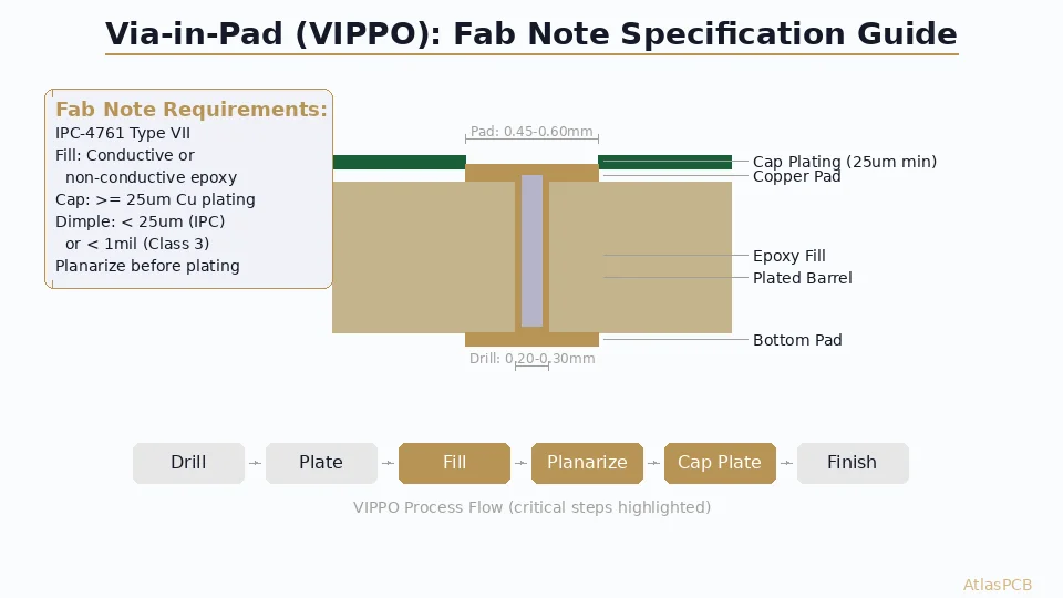
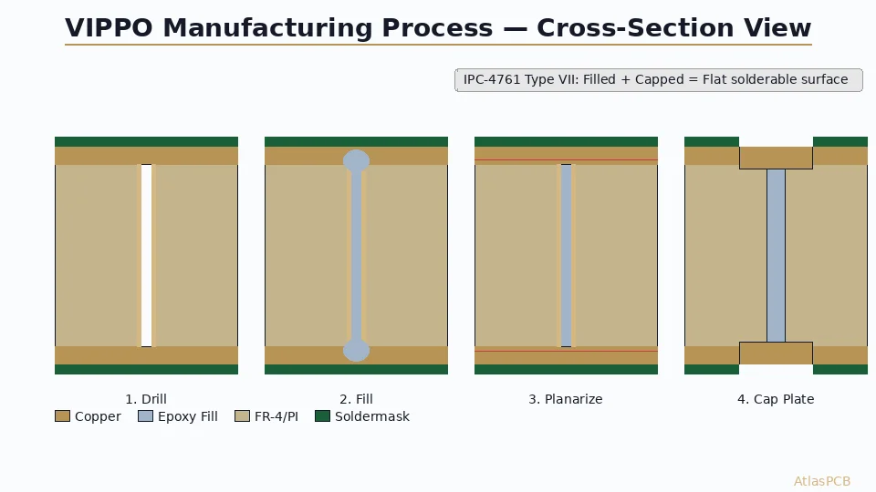
Type VII: Filled and Capped (Planar)
- Via filled with epoxy (conductive or non-conductive)
- Capped with copper plating
- Surface planarized to < 25 μm (1 mil) deviation
- Preferred for BGA via-in-pad — provides flat, reliable pad surface
Fill Material Selection
Non-Conductive Epoxy Fill (Preferred for most applications):
- Material: Peters PP2795, San-Ei SHP-9000 or equivalent
- CTE: 30-40 ppm/°C
- Tg: > 150°C
- Advantages: No risk of electrical shorting between layers, lower cost, simpler process
- Limitation: Cannot carry current through the fill; thermal conductivity lower than copper
Conductive Epoxy Fill:
- Material: Tatsuta AE3030, DuPont CB100 or equivalent
- Contains silver particles for electrical and thermal conductivity
- Advantages: Via remains electrically functional through fill, better thermal path
- Limitations: Higher cost, potential silver migration concerns, fill resistance adds to via impedance
- Use when: Via must carry current or provide thermal path (power/ground vias under thermal pad)
BGA Pad Design Rules
NSMD vs SMD Pad Configuration
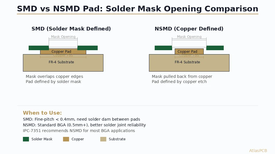
NSMD (Non-Solder Mask Defined):
Copper pad diameter = Nominal ball pad size
Solder mask opening = Copper pad + 2× mask clearance
Typical mask clearance = 50-75 μm per side
Example for 0.5 mm pitch BGA (280 μm ball pad):
- Copper pad: 280 μm diameter
- Mask opening: 280 + 2×60 = 400 μm diameter
- Copper-to-copper spacing: 500 - 280 = 220 μm (adequate for routing)
SMD (Solder Mask Defined):
Copper pad diameter = Mask opening + 2× mask overlap
Mask opening = Defines actual solder-wettable area
Typical mask overlap = 50-75 μm per side
Example for 0.4 mm pitch BGA (200 μm ball pad):
- Mask opening: 200 μm diameter
- Copper pad: 200 + 2×60 = 320 μm diameter
- But only 200 μm is wettable by solder
Pad Design Decision Matrix
| BGA Pitch | Recommended Pad | Via-in-Pad Via Size | Rationale |
|---|---|---|---|
| 1.27 mm | NSMD | 0.3 mm drill | Ample spacing for dog-bone escape |
| 1.0 mm | NSMD | 0.25 mm drill | Standard via-in-pad |
| 0.8 mm | NSMD | 0.2 mm drill | Fine pitch, 2 trace escape between pads |
| 0.65 mm | NSMD | 0.15 mm drill | HDI required for inner ball escape |
| 0.5 mm | NSMD | 0.1 mm laser | Microvia mandatory, 1 trace max between |
| 0.4 mm | NSMD or SMD | 0.075 mm laser | Ultra-fine pitch, stacked microvias |
| 0.3 mm | SMD | 0.05 mm laser | Mask registration limits NSMD |
Via Sizing for Via-in-Pad
The via in the BGA pad must be small enough to:
- Fill completely with epoxy (fill aspect ratio < 1.5:1 for reliable fill)
- Cap plate without dimple > 25 μm
- Not consume excessive pad area
Rule of thumb: Via drill diameter ≤ 50% of pad diameter
For a 0.5 mm pitch BGA with 280 μm NSMD pad:
- Maximum via drill: 280 × 0.5 = 140 μm → use 100-125 μm laser drill
- Via depth (assuming blind via): 60-100 μm core + 30 μm prepreg = 90-130 μm
- Aspect ratio: 130/100 = 1.3:1 ✓ (excellent for epoxy fill)
Complex BGA Routing? We Can Help.
AtlasPCB offers via-in-pad with IPC-4761 Type VII fill, ±1 mil cap planarization, and X-ray verified voiding < 15% for Class 3 assemblies.
Request BGA PCB Quote →Manufacturing Process for Reliable Via-in-Pad
Step-by-Step Process Flow
1. Drill Vias
- Mechanical drill for ≥ 0.2 mm; laser drill for < 0.2 mm
- Clean drill smear with plasma or desmear chemistry
- Inspect via depth and wall quality (SEM for laser vias)
2. Plate Via Barrels
- Electroless copper seed (0.5-1.0 μm)
- Electrolytic copper fill to specified thickness
- For microvias: pulse-reverse plating for void-free fill
- Panel plate or pattern plate depending on design
3. Fill Vias with Epoxy
- Screen print fill material into vias (squeegee both sides)
- Ensure > 70% fill depth (100% preferred)
- Vacuum-assist filling for aspect ratios > 1:1
- Air bubbles at this stage = voids in final product
4. Cure Epoxy
- Oven cure per material specification (typically 150°C × 60 min)
- Must achieve full cure—undercured epoxy outgasses during reflow
- Verify cure with DSC if process is new
5. Surface Planarization
- Belt sand or ceramic brush to remove fill material from surface
- Must not gouge surrounding copper
- Target: fill flush with copper surface ±10 μm
6. Cap Plating
- Electroless copper (0.5 μm seed) + electrolytic copper (15-25 μm)
- Cap must fully cover filled via with no pinholes
- Flatness specification: ±25 μm (1 mil) for BGA pads
- Inspect with profilometer or white light interferometer
7. Final Surface Finish
- ENIG, OSP, or immersion silver over cap-plated pad
- ENIG preferred for BGA: excellent coplanarity and shelf life
- Verify surface finish doesn’t create additional outgassing risk
8. Bake Before Assembly
- Pre-assembly bake: 125°C × 4 hours minimum
- Removes moisture absorbed by fill material during storage
- Critical step often skipped—leads to voiding spikes
Process Control Points
| Parameter | Target | Tolerance | Inspection Method |
|---|---|---|---|
| Fill depth | 100% | Min 70% | Cross-section, CT |
| Cap plating thickness | 20 μm | ±5 μm | Eddy current |
| Cap surface flatness | 0 μm | ±25 μm | Profilometer |
| Cap plating adhesion | > 1.0 N/mm | — | Peel test (coupon) |
| Via fill void content | 0% | Max 10% by area | CT scan |
| Post-cure Tg | Per spec | > spec - 5°C | DSC (coupon) |
Thermal Pad Design for BGA
The exposed thermal pad (die paddle) under many BGAs presents unique challenges:
Thermal Pad Voiding
Thermal pads are large (typically 3-8 mm per side), making voiding particularly problematic:
- Large area = more flux entrapment opportunity
- Solder paste printing must cover entire pad uniformly
- Voiding directly impacts thermal resistance (θjc increases proportionally)
Design Solutions for Thermal Pads
1. Windowed Solder Paste Pattern
- Instead of solid paste coverage, use a checkerboard or window pattern
- 60-75% paste coverage area with gaps for gas escape
- Stencil design: 1.0 mm squares with 0.3 mm gaps between
2. Multiple Small Vias (Not One Large Via)
- Place array of 0.3 mm filled vias on 1.0-1.27 mm pitch across thermal pad
- Each via provides thermal path to internal ground plane
- Avoid single large via or slot—impossible to fill reliably
3. Solder Mask Dam
- Create 0.15 mm solder mask dams in grid pattern across thermal pad
- Dams prevent uncontrolled solder flow during reflow
- Define discrete solder reservoirs that trap less gas
4. Vapor Phase Reflow
- Significantly reduces voiding vs. convection reflow for thermal pads
- Uniform heating eliminates temperature gradients that trap flux
- Recommended for Class 3 assemblies with large thermal pads
Inspection and Acceptance Criteria
X-Ray Inspection for BGA Voiding
2D X-ray imaging is the primary inspection method for BGA voids:
- Voiding appears as lighter areas within the darker solder joint circle
- Image analysis software calculates void percentage per ball
- Statistical sampling per IPC-7095: check 100% of Class 3, sample for Class 2
Void Measurement Methodology
Per IPC-7095D:
- Capture X-ray image at 0° incidence (perpendicular to board)
- Define region of interest (ROI) as the solder ball boundary
- Threshold to identify void areas (lighter pixels) within ROI
- Calculate: Void % = (Total void area / Total pad area) × 100
Acceptance Criteria Summary
| Class | Max Void % per Joint | Max Single Void | Process Action |
|---|---|---|---|
| Class 1 (consumer) | 30% | — | None required |
| Class 2 (dedicated service) | 25% | — | SPC monitoring |
| Class 3 (high reliability) | 25% | < 10% of pad ∅ | 100% inspect |
| Thermal pad (all classes) | 25% | < 15% of pad area | X-ray 100% |
CT Scanning for Critical Applications
For aerospace, medical, and automotive ADAS applications, 3D CT scanning provides:
- True volumetric void measurement (vs. 2D projection)
- Identification of void position within joint (top/bottom/center)
- Detection of head-in-pillow defects obscured in 2D X-ray
- Verification of via fill quality beneath cap plating
Common Failure Modes and Troubleshooting
High Voiding After Via-in-Pad Implementation
Symptom: Voiding jumps from 5-10% (dog-bone routing) to 30-50% after switching to via-in-pad.
Root Causes (in order of likelihood):
- Incomplete via fill (< 70% depth) — inspect cross-sections
- Missing or inadequate pre-assembly bake — add 125°C/4hr step
- Cap plating pinholes — verify with dye penetrant test
- Undercured fill epoxy — verify DSC against specification
- Fill material incompatible with reflow temperature — check Td
Asymmetric Voiding Pattern
Symptom: One side/corner of BGA consistently shows higher voiding.
Root Causes:
- Paste volume variation (stencil aperture issue or printer offset)
- Board warp creating inconsistent paste transfer
- Reflow temperature gradient across board
- Solder mask registration shift exposing partial via on some pads
Voiding Only on Inner Ball Rows
Symptom: Perimeter balls fine, inner balls show high voiding.
Root Causes:
- Inner balls have via-in-pad, perimeter balls don’t
- Inner area has longer outgassing path (gases trapped by surrounding molten balls)
- Profile needs longer soak to fully volatilize flux before melt
- Consider extended time-above-liquidus: 60-90s (vs typical 45-60s)
Design for Manufacturability Checklist
Before releasing your BGA/via-in-pad design, verify:
- Via drill size ≤ 50% of pad diameter
- Fill aspect ratio ≤ 1.5:1 (depth:diameter)
- IPC-4761 Type VII specified in fabrication notes
- Cap plating flatness ±1 mil called out
- NSMD pads specified for pitch ≤ 0.5 mm
- Solder mask registration tolerance achieves required pad-to-mask clearance
- Thermal pad has windowed paste pattern defined in assembly drawing
- Pre-assembly bake requirement noted on assembly drawing
- X-ray inspection criteria defined in test specification
- Coupon for cross-section verification included in panel design
- Stencil thickness specified (typically 4-5 mil for 0.5 mm pitch BGA)
- Paste volume calculation verified (< 60% transfer ratio for fine pitch)
Conclusion: Reliable BGA Assembly Starts with PCB Design
Preventing BGA solder voiding isn’t about one magic fix—it’s about systematic design and process control from PCB layout through final inspection. The via-in-pad technique, when properly implemented with IPC-4761 Type VII fill and cap plating, enables routing density that would be impossible with dog-bone fanout while maintaining voiding levels well below IPC acceptance limits.
The key takeaways:
- Fill quality is everything—specify and verify > 70% fill depth
- Cap plating must be pinhole-free and planar (±1 mil)
- NSMD pads win for pitch ≤ 0.5 mm reliability
- Bake before assembly—the most-skipped, most-impactful step
- Work with your fabricator early—via-in-pad capability varies enormously between shops
Designing a high pin-count BGA PCB? AtlasPCB’s DFM review service includes via-in-pad fill analysis, pad design verification against IPC-7095, and cross-section validation on first articles. Get a quote with DFM support included.
Further Reading
- [Via-in-Pad Design: Filled, Capped, and Plated Over — Complete Guide]/blog/via-in-pad-design/)
- [PCB Thermal Management: Heat Dissipation Techniques for Reliable Electronics]/blog/pcb-thermal-management/)
- [Press-Fit Via Design for PCB Connectors: Hole Sizing, Plating & IPC Compliance]/blog/pcb-press-fit-via-design/)
- [PCB Copper Plating Process: Electroless vs Electrolytic Copper for HDI Vias and High-Density Interconnects]/blog/pcb-copper-plating-electroless-vs-electrolytic-hdi-vias/)
- [PCB Via Reliability Testing: IST, Thermal Cycling, and IPC-6012 Compliance for Microvias]/blog/pcb-via-reliability-testing/)
- HDI PCB Manufacturing
About AtlasPCB — We specialize in complex PCB manufacturing for HDI, RF, and high-reliability applications. Explore our HDI PCB manufacturing capabilities, PCB assembly services, or get an free engineering DFM review . Every order includes free engineering review. Get your quote.
Reviewed by AtlasPCB Engineering Team — IPC-certified manufacturing specialists with 15+ years of production experience in HDI, RF, and high-reliability PCB fabrication. Content based on factory floor data and real customer design reviews.
- BGA
- via-in-pad
- solder voiding
- pad design
- NSMD
- SMD
- PCB assembly
- fine-pitch BGA
- IPC-7095
- DFM