· AtlasPCB Engineering · Engineering · 8 min read
PCB Stackup Symmetry: Why Balanced Lamination Prevents Warpage in Multilayer Boards
Learn why stackup symmetry is critical for multilayer PCB reliability. This guide covers balanced lamination rules, CTE-driven warpage mechanisms, copper balancing techniques, and IPC-6012 bow/twist specifications with practical stackup examples.

The Cost of Ignoring Stackup Symmetry
A multilayer PCB that looks perfect in the EDA tool can warp catastrophically during assembly. When the board enters the reflow oven at 245–260°C, asymmetric internal stresses cause the panel to bow, twist, or develop a potato-chip shape that makes component placement impossible. For BGAs with 0.4 mm pitch, even 0.5% bow exceeds the co-planarity budget, causing open solder joints.
The root cause in most cases: an unbalanced stackup. The designer focused on signal routing, impedance targets, and layer count — but forgot to mirror the construction about the board’s center axis.
This guide explains the physics behind stackup-induced warpage, provides concrete rules for balanced lamination design, and shows how to verify symmetry before sending your files to the fabricator.
How Lamination Creates Internal Stress
The Press Cycle
A multilayer PCB is built by stacking copper-clad cores and prepreg sheets, then pressing them together under heat and pressure. During the lamination press cycle:
- Heat-up phase (25°C → 180°C): All materials expand. The resin in prepreg sheets melts and flows, filling gaps around copper features.
- Cure phase (180°C, 60–90 min): The resin cross-links and hardens, locking all layers into a rigid structure.
- Cool-down phase (180°C → 25°C): All materials contract. But they don’t contract equally.
The problem: copper has a CTE of ~17 ppm/°C, FR-4 resin has ~60 ppm/°C in the Z-axis (through-thickness), and glass fiber has ~5 ppm/°C in the XY plane. During cool-down, these different contraction rates create residual stresses locked into the laminate.
Why Symmetry Cancels Stress
In a symmetric stackup, identical materials and thicknesses exist above and below the center axis. During cool-down, the residual stresses on the top half are mirror-images of the bottom half. These equal and opposite forces cancel each other, and the board remains flat.
In an asymmetric stackup, the forces are unbalanced. One half contracts more than the other, and the board bends toward the side with greater contraction. This is the fundamental mechanism behind lamination-induced warpage.
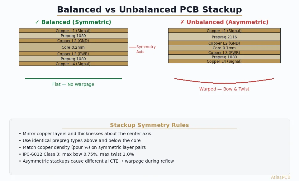
The Three Dimensions of Stackup Symmetry
Achieving a truly balanced stackup requires symmetry in three dimensions:
1. Material Symmetry
Every core and prepreg layer above the center must have a matching layer below the center with identical material properties.
Rules:
- Same resin system (e.g., both Tg170 FR-4, or both Megtron 6)
- Same glass style (e.g., both 1080 or both 2116)
- Same core/prepreg type in the mirror position
- For [hybrid stackups with Rogers and FR-4]/blog/pcb-hybrid-stackup-rogers-fr4/): place Rogers layers symmetrically about the center
Example — 8-layer symmetric stackup:
| Position | Layer | Material | Thickness |
|---|---|---|---|
| Top | L1 Signal | Copper 1oz | 35 μm |
| Prepreg | 2×1080 | 0.13 mm | |
| L2 GND | Copper 0.5oz | 17.5 μm | |
| ↑ | Core | FR-4 | 0.2 mm |
| Center → | L3 Signal | Copper 0.5oz | 17.5 μm |
| Prepreg | 2×1080 | 0.13 mm | |
| ↓ | L4 PWR | Copper 0.5oz | 17.5 μm |
| Core | FR-4 | 0.2 mm | |
| L5 PWR | Copper 0.5oz | 17.5 μm | |
| Prepreg | 2×1080 | 0.13 mm | |
| L6 Signal | Copper 0.5oz | 17.5 μm | |
| Core | FR-4 | 0.2 mm | |
| L7 GND | Copper 0.5oz | 17.5 μm | |
| Prepreg | 2×1080 | 0.13 mm | |
| Bottom | L8 Signal | Copper 1oz | 35 μm |
Notice the mirror: L1↔L8 (same copper weight), L2↔L7 (both GND planes, same copper), L3↔L6 (signal layers), L4↔L5 (power layers). Prepreg and cores are identical in mirror positions.
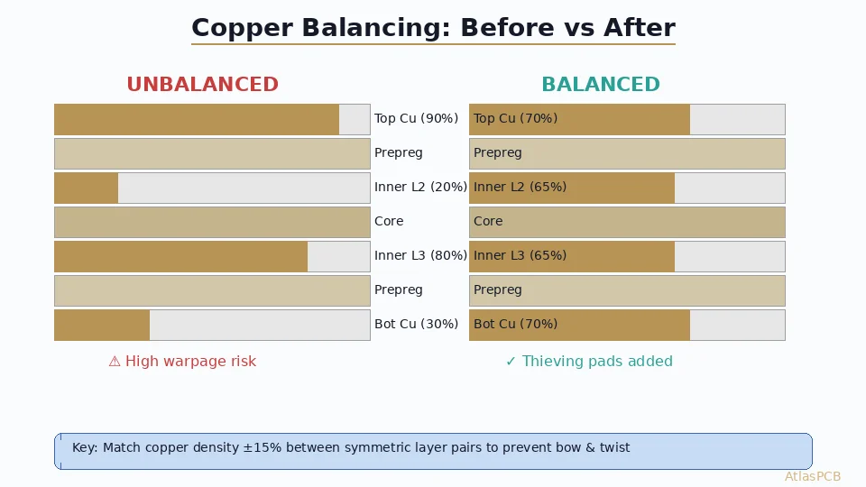
2. Copper Density Symmetry
Even with perfectly symmetric materials, different copper coverage on mirror layers creates imbalance. A solid ground plane (90%+ copper) mirrors a sparse signal layer (30% copper) = trouble.
Copper density creates asymmetric CTE because:
- High copper content → lower in-plane CTE (copper restrains resin expansion)
- Low copper content → higher in-plane CTE (resin-dominated behavior)
- Different CTE on mirror layers → differential contraction during cool-down → warpage
Rules:
- Measure copper density on each layer using your EDA tool’s area calculator
- Compare mirror pairs: L1 vs L8, L2 vs L7, etc.
- Target < 15% density difference between mirror pairs for Class 3
- Target < 25% density difference for Class 2
Copper balancing techniques when the design is inherently asymmetric:
- Add copper pour (ground fill) to sparse signal layers
- Use [copper thieving patterns]/blog/pcb-copper-balancing-techniques/) in unused areas
- Add cross-hatch ground fill (reduces density more predictably than solid pour)
- On internal power planes, use thermal relief patterns that achieve consistent copper percentage
3. Thickness Symmetry
The total dielectric thickness above the center must equal the total below. This applies to both individual layer pairs and the cumulative stackup.
Common violations:
- Using 2×1080 prepreg on one side and 1×2116 on the other (different resin content even if similar thickness)
- Different core thicknesses in mirror positions
- Adding an extra adhesive layer for a [rigid-flex section]/blog/rigid-flex-pcb-design-bend-radius-reliability-guide/) on only one side
Need a Balanced Stackup for Your Multilayer PCB?
AtlasPCB's engineering team designs symmetric stackups optimized for impedance, warpage, and manufacturing yield — free with every order.
Get a Free Stackup Review →IPC-6012 Bow and Twist Specifications
Class-Based Limits
IPC-6012 defines maximum allowable bow and twist as a percentage of board diagonal:
| Parameter | Class 1 | Class 2 | Class 3 |
|---|---|---|---|
| Bow | 1.5% | 1.5% | 0.75% |
| Twist | 1.5% | 1.5% | 1.0% |
Bow is a uniform curvature (the board curves like a cylinder). Twist is a non-planar deformation (opposite corners lift — the potato chip shape).
For a 200 mm × 100 mm board (diagonal = 224 mm):
- Class 3 max bow = 224 × 0.75% = 1.68 mm
- Class 3 max twist = 224 × 1.0% = 2.24 mm
These limits apply after reflow — the board must remain within spec even after experiencing assembly temperatures.
Measurement Method
Per IPC-TM-650, Method 2.4.22:
- Place the board on a flat granite surface
- Measure the maximum gap between the board and surface at multiple points
- Calculate percentage: (max gap / diagonal length) × 100%
Post-Reflow Warpage Increase
A board that passes bow/twist inspection as-fabricated may fail after reflow. Typical warpage increase during lead-free reflow:
- Symmetric stackup: 0.1–0.2% increase
- Mildly asymmetric: 0.3–0.5% increase
- Severely asymmetric: 0.5–1.0%+ increase
This is why IPC-6012 Class 3 requires low initial warpage — it must accommodate the reflow-induced increase and still remain within spec.
Practical Stackup Examples
4-Layer Balanced Stackup
The simplest balanced multilayer. The center core provides the symmetry axis.
| Layer | Function | Cu Weight | Material | Thickness |
|---|---|---|---|---|
| L1 | Signal/Component | 1 oz | — | 35 μm |
| — | Prepreg | — | 1×2116 | 0.12 mm |
| L2 | GND | 1 oz | — | 35 μm |
| — | Core (center) | — | FR-4 | 0.8 mm |
| L3 | PWR | 1 oz | — | 35 μm |
| — | Prepreg | — | 1×2116 | 0.12 mm |
| L4 | Signal/Component | 1 oz | — | 35 μm |
Symmetry check: L1↔L4 (both signal, same copper), L2↔L3 (both plane, same copper), prepreg identical above and below the core. ✓
10-Layer Balanced Stackup
More layers require careful attention to both core and prepreg placement.
| Layer | Function | Cu Weight | Material | Thickness |
|---|---|---|---|---|
| L1 | Signal | 1 oz | — | 35 μm |
| — | Prepreg | — | 1×1080+1×2116 | 0.15 mm |
| L2 | GND | 0.5 oz | — | 17.5 μm |
| — | Core | — | FR-4 | 0.15 mm |
| L3 | Signal | 0.5 oz | — | 17.5 μm |
| — | Prepreg | — | 1×1080 | 0.075 mm |
| L4 | PWR | 0.5 oz | — | 17.5 μm |
| — | Core | — | FR-4 | 0.15 mm |
| L5 | Signal | 0.5 oz | — | 17.5 μm |
| — | — | Center Axis | — | — |
| L6 | Signal | 0.5 oz | — | 17.5 μm |
| — | Core | — | FR-4 | 0.15 mm |
| L7 | PWR | 0.5 oz | — | 17.5 μm |
| — | Prepreg | — | 1×1080 | 0.075 mm |
| L8 | Signal | 0.5 oz | — | 17.5 μm |
| — | Core | — | FR-4 | 0.15 mm |
| L9 | GND | 0.5 oz | — | 17.5 μm |
| — | Prepreg | — | 1×1080+1×2116 | 0.15 mm |
| L10 | Signal | 1 oz | — | 35 μm |
Mirror pairs: L1↔L10, L2↔L9, L3↔L8, L4↔L7, L5↔L6. All prepreg and core materials are identical in mirror positions. ✓
When Perfect Symmetry Is Impossible
Some designs fundamentally resist symmetry:
- Rigid-flex boards: The flex region has different construction than the rigid region
- Metal-core boards: The metal core is offset from center for thermal reasons
- Embedded components: Active/passive devices embedded in specific layers
Mitigation strategies:
- Achieve the best symmetry possible in the non-constrained layers
- Use [warpage simulation]/blog/multilayer-pcb-warpage-simulation/) to predict deflection and adjust prepreg selection
- Add copper balancing and thieving on the lighter side
- Specify tighter lamination press parameters (temperature uniformity, pressure distribution)
- Consider post-lamination baking to relieve residual stress
Copper Balancing Techniques in Detail
Ground Pour / Copper Fill
The most common technique. Add copper pour connected to the ground net on sparse signal layers.
Best practices:
- Use 0.2–0.3 mm clearance to signal traces (avoid impedance disturbance)
- Connect pour to ground with thermal reliefs, not solid connections, near via pads
- Verify that added pour doesn’t create unwanted capacitance on [high-speed differential pairs]/blog/differential-pair-routing-rules-high-speed-serdes-pcb/)
Copper Thieving
Non-connected copper patterns placed in unused areas. Used when ground pour would create signal integrity problems.
Pattern options:
- Dot array: 0.5–1.0 mm diameter dots on 1.5–2.0 mm pitch
- Cross-hatch: 0.15 mm lines on 0.5 mm pitch
- Solid rectangles: 2×2 mm pads in open areas
Dummy Copper Features
For layers where neither ground pour nor thieving is possible (e.g., inner signal layers with strict crosstalk requirements):
- Add copper features outside the board outline but within the panel frame
- These contribute to copper balance during lamination even though they’re removed during routing
Verification Workflow
Before Sending to Fab
- Export copper density report from your EDA tool for each layer
- Calculate mirror pair differences:
- |L1_density - LN_density| < 15% ✓
- |L2_density - L(N-1)_density| < 15% ✓
- Continue for all pairs
- Verify material symmetry in the stackup table
- Run warpage simulation for Class 3 designs or boards thinner than 1.0 mm
- Check with fabricator: Request their [standard stackup offerings]/blog/pcb-stackup-design-guide/) — many fabs have pre-qualified symmetric stackups that have proven warpage performance
During Fabrication
Request the fabricator to:
- Measure bow/twist on a panel sample before shipping
- Provide post-reflow simulation or characterization data
- Use balanced copper distribution in the panel border (frame copper)
- Apply uniform lamination pressure across the panel
Design Checklist for Balanced Stackups
Before finalizing your stackup, verify each item:
- All prepreg layers have identical mirror partners (same glass style and count)
- All core layers have identical mirror partners (same material and thickness)
- Copper weight is identical on mirror layer pairs
- Copper density difference < 15% on each mirror pair
- [High-Tg material]/blog/high-tg-pcb-material-selection/) used if peak reflow > 250°C
- No mixed material types without symmetric placement
- Total stackup thickness matches fabricator’s preferred range
- Impedance calculations verified with the symmetric stackup dimensions
- Fabricator confirmed the stackup is achievable in their press
Further Reading
- [PCB Bow and Twist Specification]/blog/pcb-bow-and-twist-specification/) — Detailed IPC bow/twist measurement methods
- [Multilayer PCB Warpage Simulation]/blog/multilayer-pcb-warpage-simulation/) — FEA-based warpage prediction
- [PCB Stackup Design Guide]/blog/pcb-stackup-design-guide/) — General stackup design principles
- [High-Layer Count PCB Challenges]/blog/high-layer-count-pcb-challenges/) — Managing complexity in 12+ layer boards
- [Controlled Impedance PCB Stackup Design Rules]/blog/controlled-impedance-pcb-stackup-design-rules/) — Impedance-first stackup design
Struggling with warpage on your multilayer design? AtlasPCB’s engineers review every stackup for symmetry, impedance, and manufacturability — before fabrication begins. Upload your stackup for a free review →
About AtlasPCB — We specialize in complex PCB manufacturing for HDI, RF, and high-reliability applications. Explore our multilayer PCB fabrication up to 30 layers, PCB assembly services, or get an full PCB manufacturing capabilities . Every order includes free engineering review. Get your quote.
Reviewed by AtlasPCB Engineering Team — IPC-certified manufacturing specialists with 15+ years of production experience in HDI, RF, and high-reliability PCB fabrication. Content based on factory floor data and real customer design reviews.
- stackup-design
- warpage
- lamination
- multilayer-pcb
- ipc-6012
- copper-balance
- bow-and-twist
- reflow
- reliability