· AtlasPCB Engineering · Engineering · 8 min read
SMD vs NSMD Pad Design: How to Specify Solder Mask Openings for BGA and Fine-Pitch Components
Complete engineering guide to solder mask defined (SMD) vs non-solder mask defined (NSMD) pad design for BGA, QFN, and fine-pitch components. Covers pad geometry rules, IPC-7351 guidelines, thermal fatigue life comparison, solder joint reliability data, and how to specify mask openings in your Gerber output.
Quick Decision: NSMD for Most BGA, SMD for Ultra-Fine Pitch
For the engineer about to generate Gerber files: if your BGA pitch is 0.5mm or larger, use NSMD pads. This is the IPC-7351 recommended default and provides the best solder joint reliability. The table below summarizes the decision boundary.
| BGA Pitch | Recommended Pad Type | Reason |
|---|---|---|
| 0.8mm+ | NSMD | Standard, best reliability |
| 0.5mm | NSMD | Adequate solder dam (>100 µm) |
| 0.4mm | NSMD or SMD | Fabricator-dependent, verify dam width |
| 0.35mm | SMD | Solder dam too thin for NSMD |
| 0.3mm | SMD | Only viable option at this density |
The Engineering Basis: Why Pad Definition Method Affects Reliability
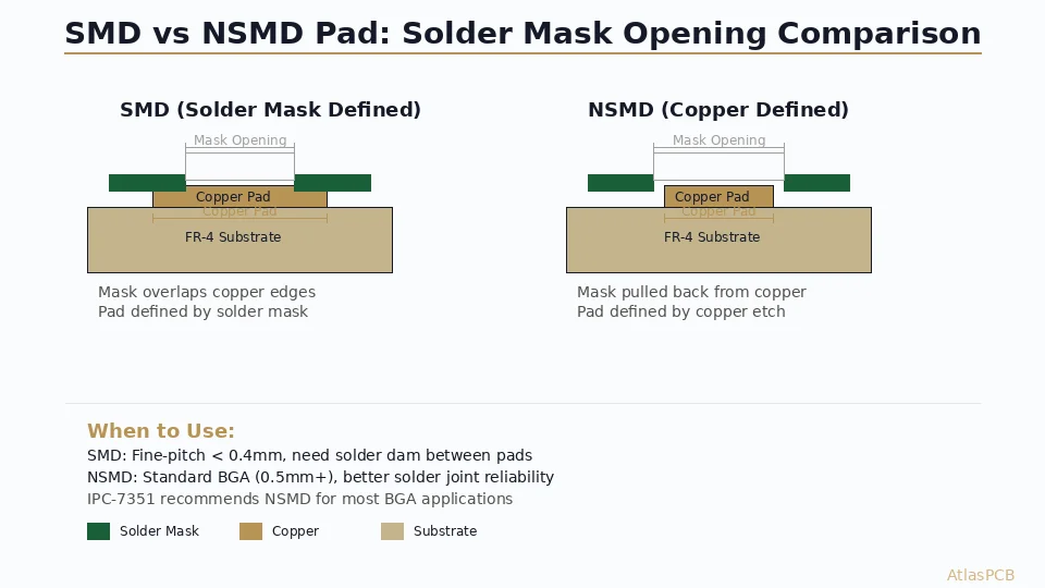
The distinction between SMD and NSMD seems like a minor fabrication detail, but it fundamentally changes the solder joint geometry — and geometry drives fatigue life. When a BGA package thermally cycles between operating temperature and ambient, the CTE mismatch between silicon die (2.6 ppm/C), package substrate (12-16 ppm/C), and PCB (14-17 ppm/C in-plane) creates cyclic shear strain on every solder ball. The joint’s ability to survive this strain depends directly on its geometric compliance.
With NSMD pads, the solder wets around the exposed copper sidewalls, forming a barrel or hourglass shape. This geometry distributes the stress concentration away from the critical intermetallic layer at the pad interface. The additional wettable surface area — typically 15-20% more than an SMD pad of the same nominal diameter — creates a more gradual transition from solder to copper, reducing the peak strain at the failure initiation point.
SMD pads, by contrast, create a flat-bottomed joint profile. The solder mask lip acts as a geometric stress concentrator where it meets the solder fillet, and the reduced wettable area concentrates all thermal strain across a smaller interfacial cross-section. Published reliability data consistently shows NSMD joints lasting 1.5-3x more thermal cycles before crack propagation reaches critical length.
However, SMD pads have one significant advantage: pad dimensional control. Solder mask registration (typically +/-25 µm on LDI systems) is tighter than copper etch tolerance (+/-25-50 µm depending on copper weight and feature size). At ultra-fine pitches where pad-to-pad spacing is less than 100 µm, the etch tolerance of NSMD pads can cause bridging or insufficient clearance. The mask-defined approach removes copper etch variation from the equation.

BGA DESIGN REVIEW
Fine-Pitch BGA Layout? We Verify Your Pad Geometry
Our DFM analysis checks solder dam widths, pad-to-mask registration, and recommends SMD or NSMD based on your specific BGA pitch and our process capabilities.
Upload Design for Review ›How to Specify Mask Openings in Your Gerber Output
The solder mask layer in your Gerber package defines where mask is removed (openings), not where it is applied. Getting the pad/mask relationship correct requires understanding three parameters: copper pad diameter, mask opening diameter, and the resulting mask expansion or overlap.
For NSMD pads, the mask opening must be larger than the copper pad. The standard expansion is 50-75 µm (2-3 mil) per side beyond the copper edge. So for a 0.30mm copper pad on a 0.5mm-pitch BGA, the mask opening should be 0.36-0.38mm. This provides adequate clearance for mask registration tolerance while ensuring the copper sidewalls are fully exposed for solder wetting. In your CAD tool, this appears as a positive mask expansion value in the pad stack definition.
For SMD pads, the mask opening is smaller than the copper pad. The overlap is typically 50-75 µm per side. A 0.30mm mask opening on a 0.35mm copper pad gives 25 µm overlap per side. The copper pad is intentionally oversized to account for mask registration variation — even at worst-case misregistration, the mask still overlaps the copper edge.
The critical Gerber output check: verify your solder mask layer shows correct polarity (openings, not coverage) and that the pad/mask relationship matches your design intent. Many CAD tools default to a global mask expansion rule — override this for BGA arrays where you have explicitly chosen SMD vs NSMD geometry. Export your mask layer and copper layer, overlay them in your Gerber viewer, and visually verify the pad-to-mask relationship before submitting for fabrication.
One common error that causes expensive re-spins: applying a blanket 3-mil mask expansion across the entire board including fine-pitch BGA arrays. At 0.4mm pitch, a 3-mil expansion per side consumes the entire solder dam, leaving zero mask between adjacent pads. The fabricator will either reject the file or expand the pads to minimum dam — neither outcome matches your design intent. Always set BGA pad mask expansion explicitly in the pad stack, separate from the global rule.
HDI CAPABILITIES
50 µm Solder Dam? We Handle Fine-Pitch BGA Routinely
LDI solder mask with 50 µm minimum dam width. Via-in-pad VIPPO for BGA fanout. Proven process for 0.4mm pitch and below.
Real-World Scenarios: When the Choice Gets Complicated
The straightforward cases — 0.8mm BGA with NSMD, 0.3mm with SMD — are easy. The engineering judgment comes in the grey zone around 0.4-0.5mm pitch where both approaches are viable but trade different failure modes.
Mixed-pitch boards present the most common dilemma. A design might have a 0.5mm-pitch application processor, a 0.4mm-pitch DDR memory stack, and multiple 0.65mm-pitch power management ICs. Applying a single pad definition across all packages is suboptimal. The better approach: NSMD for the 0.5mm+ packages (maximize reliability) and SMD for the 0.4mm packages (ensure dam integrity). This does require verifying that your fabricator can handle both pad definition types on the same layer — some shops prefer uniformity for process simplicity.
Thermal pad mask design is another area where the SMD/NSMD choice matters. Exposed thermal pads on QFN and LGA packages should typically use SMD definition with solder mask covering 25-30% of the thermal pad area in a window-pane pattern. This controls solder paste volume and prevents package floating during reflow. The mask segments also provide void escape channels. An NSMD thermal pad allows excessive solder volume that causes voiding and component tilt.
For boards destined for automotive qualification (AEC-Q100), the pad definition directly impacts JEDEC thermal cycling results. NSMD pads are strongly recommended for automotive BGA connections because the 2-3x fatigue life improvement often makes the difference between passing and failing the mandated 1000-cycle thermal shock requirement. Several automotive OEMs now specify NSMD as a design requirement in their component application notes.
AUTOMOTIVE PCB EXPERTISE
Building for Automotive Reliability Standards?
We manufacture to IPC Class 3/3A with controlled pad definition for automotive thermal cycling requirements. IATF 16949 quality management.
Request Automotive Quote ›Design Checklist: Before You Output Gerbers
Use this checklist to verify your solder mask design before exporting for fabrication:
- Confirm pad definition type (SMD or NSMD) for each BGA/QFN component
- Calculate solder dam width: (pitch - mask opening) for NSMD, or (pitch - copper pad) for SMD
- Verify minimum dam exceeds 75 µm (or 50 µm if your fabricator confirms capability)
- Set BGA-specific mask expansion in pad stack — do not rely on global rule
- Check thermal pad mask pattern (window-pane for QFN/LGA)
- Overlay mask and copper in Gerber viewer — verify intent visually
- Note pad definition type in fab drawing (“NSMD per IPC-7351” or “SMD per component vendor spec”)
ATLASPCB
Upload Your Design — We Check Pad/Mask Geometry Automatically
Our automated DFM system flags solder dam violations, incorrect pad definitions, and mask registration concerns. Get feedback before committing to production.
Get Instant Quote ›Related Reading:
About AtlasPCB — We specialize in complex PCB manufacturing for HDI, RF, and high-reliability applications. Explore our HDI PCB manufacturing capabilities, free engineering DFM review, or get an full PCB manufacturing capabilities . Every order includes free engineering review. Get your quote.
Reviewed by AtlasPCB Engineering Team — IPC-certified manufacturing specialists with 15+ years of production experience in HDI, RF, and high-reliability PCB fabrication. Content based on factory floor data and real customer design reviews.
- solder mask
- BGA
- NSMD
- SMD pad
- DFM
- fine-pitch