· AtlasPCB Engineering · Engineering · 8 min read
Metal Core PCB (MCPCB) Design Guide: Thermal Management for LED and Power Electronics
Comprehensive design guide for Metal Core PCBs (MCPCBs) covering aluminum and copper core substrates, dielectric layer selection, thermal resistance calculations, single-layer vs multilayer MCPCB architectures, and DFM guidelines for LED lighting, power converters, and motor drive applications.
Introduction: The Thermal Problem in Power Electronics
Every electronic component generates waste heat. For low-power circuits (microcontrollers, sensors, communication ICs), standard FR-4 PCBs dissipate heat adequately through copper planes and convection.
But high-power components create thermal densities that overwhelm organic substrates:
- High-brightness LEDs: 3–15 W per device, junction temperature must stay below 120°C for rated lifetime (50,000+ hours)
- Power MOSFETs/IGBTs: 10–500 W per device in motor drives and inverters
- Voltage regulators: 5–50 W switching converters in space-constrained designs
- RF power amplifiers: 10–100 W GaN/LDMOS devices for base stations
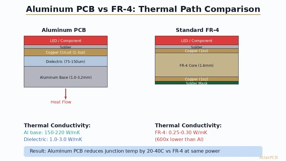
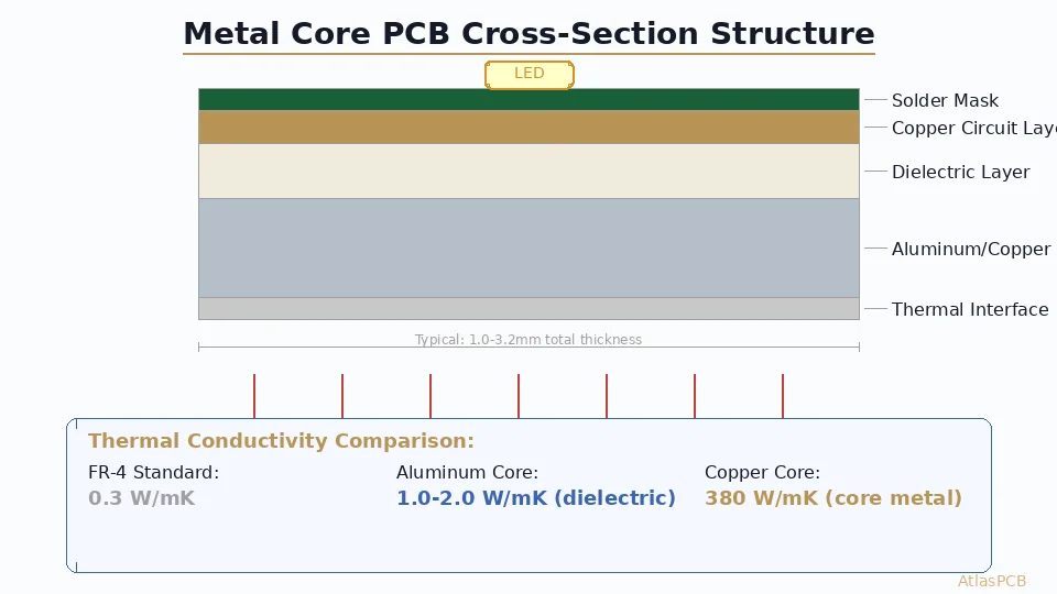
FR-4’s thermal conductivity is only 0.3 W/mK — acting as a thermal insulator rather than a heat path. Even with thermal vias (achieving equivalent conductivity of 2–4 W/mK in the via field), organic PCBs struggle to maintain acceptable junction temperatures for high-power devices.
Metal Core PCBs (MCPCBs) — also called Insulated Metal Substrates (IMS) — solve this by replacing the organic core with a thermally conductive metal plate, providing a direct low-resistance thermal path from the component to the heat sink.
MCPCB Construction
Single-Layer MCPCB (Most Common)
The standard MCPCB stackup from top to bottom:
- Solder mask (25–35 μm): Standard LPI solder mask, white for LED applications
- Copper circuit layer (35–105 μm / 1–3 oz): Standard etched copper traces
- Dielectric insulation layer (75–200 μm): Thermally conductive, electrically insulating polymer-ceramic composite
- Metal core (0.8–3.2 mm): Aluminum alloy or copper plate
- Optional: back-side finish: Anodization, plating, or thermal interface material pre-applied
The Dielectric Layer: Critical Bottleneck
The dielectric layer is simultaneously the most critical and most challenging component of MCPCB design. It must provide:
- Electrical isolation: 2–8 kV/mm breakdown voltage (safety requirement)
- Thermal conduction: 1–7 W/mK (performance requirement)
- Adhesion: Bond strength to both copper foil and metal core
- CTE compliance: Accommodate differential expansion between copper and aluminum
Standard dielectric formulations use epoxy or polyimide matrices filled with thermally conductive ceramic particles (Al₂O₃, BN, or AlN). Higher filler loading increases thermal conductivity but reduces breakdown strength and adhesion.
| Dielectric Grade | Thermal Conductivity | Breakdown Voltage | Typical Use |
|---|---|---|---|
| Standard | 1.0–1.5 W/mK | 4–6 kV/mm | General LED |
| Enhanced | 2.0–3.0 W/mK | 3–5 kV/mm | High-power LED, MOSFET |
| Premium | 3.0–5.0 W/mK | 2–4 kV/mm | Power modules, IGBT |
| Ultra-high | 5.0–7.0 W/mK | 2–3 kV/mm | Laser diode, CPV |
Metal Core Options
Aluminum alloys (most common):
- 5052-H32: Good thermal conductivity (138 W/mK), excellent corrosion resistance, standard for outdoor LED fixtures
- 6061-T6: Higher strength (276 MPa yield), machinability for CNC heat sink integration, 167 W/mK
- 1060 pure aluminum: Maximum thermal conductivity (234 W/mK) but softer — used for indoor applications without mechanical stress
Copper alloys (high-performance):
- C110 (ETP copper): 385 W/mK, for maximum thermal performance in power modules
- C194 (copper-iron alloy): 260 W/mK with superior mechanical properties for automotive
- CPC (Copper-Polymer-Copper): Sandwich construction reducing weight while maintaining thermal path
Thermal Analysis and Calculation
Thermal Resistance Model
MCPCB thermal performance is characterized by junction-to-ambient thermal resistance (θ_JA):
θ_JA = θ_JC + θ_CS + θ_SA
Where:
- θ_JC = Junction-to-case resistance (component datasheet value)
- θ_CS = Case-to-sink resistance (MCPCB contribution)
- θ_SA = Sink-to-ambient resistance (heat sink + convection)
The MCPCB’s contribution (θ_CS) consists of:
θ_CS = t_Cu/(k_Cu × A) + t_diel/(k_diel × A) + t_core/(k_core × A)
Where t = thickness, k = thermal conductivity, A = heat spreading area
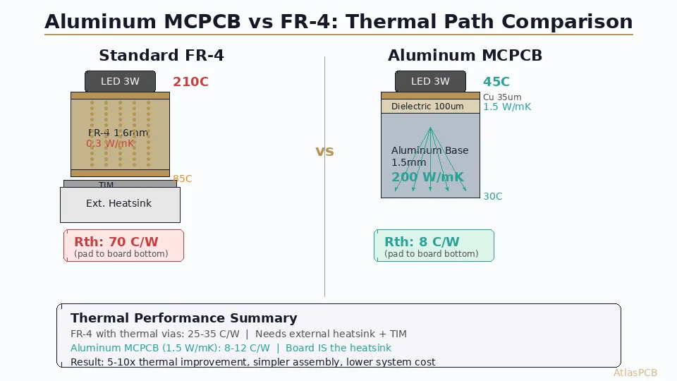
Practical Example: 10W LED on MCPCB
For a 10W LED (4×4 mm thermal pad) on standard 1.6mm aluminum MCPCB:
- Copper layer (35 μm): θ = 0.035/(386 × 16×10⁻⁶) = 0.006 °C/W (negligible)
- Dielectric (100 μm, 2 W/mK): θ = 0.1/(2 × 16×10⁻⁶) = 3.1 °C/W (dominant)
- Aluminum core (1.5 mm): θ = 1.5/(167 × 16×10⁻⁶) = 0.56 °C/W
Total θ_CS ≈ 3.7 °C/W → With 10W dissipation, ΔT = 37°C across the MCPCB
Compare to FR-4 with thermal vias:
- FR-4 (1.6mm, effective 2 W/mK with via field): θ = 1.6/(2 × 16×10⁻⁶) = 50 °C/W
- ΔT = 500°C — catastrophically impossible!
This 13× improvement in thermal resistance is why MCPCBs are mandatory for high-power LEDs.
Heat Spreading Benefit
The metal core provides lateral heat spreading that significantly increases the effective heat transfer area. For a 4×4 mm LED pad on 1.5 mm aluminum, the heat spreads outward at approximately 45° through the metal core, creating an effective transfer area of ~100 mm² at the bottom surface (vs. 16 mm² at the component) — a 6× area multiplication that further reduces θ_SA.
MCPCB Manufacturing Solutions
AtlasPCB offers aluminum and copper core MCPCBs with dielectric conductivity up to 5 W/mK — optimized for your thermal requirements.
Design Guidelines for MCPCB
Copper Circuit Layer Rules
- Minimum trace width: 150 μm (6 mil) standard — wider than typical FR-4 minimum due to etching on thick copper
- Minimum spacing: 200 μm (8 mil) for 1 oz copper; increase to 300 μm for 2–3 oz
- Thermal pad design: Maximize pad area under power components; solder mask opening = component pad + 0.1 mm per side
- No through-holes to metal core: Standard MCPCBs are single-layer; if you need grounding to core, use dedicated “thermal via” structures (dielectric removed locally)
Dielectric Design Considerations
- Uniform thickness: Variation >±10% creates thermal hotspots and voltage withstand weak points
- Thermal via option: Some manufacturers offer “direct thermal path” technology — local removal of dielectric under thermal pads, with a thin metallization barrier providing minimal electrical isolation while maximizing thermal transfer
- Voltage isolation: For SELV (Safety Extra Low Voltage) circuits (<60V), standard 75 μm dielectric is adequate. For mains-connected circuits (>250V), specify 150+ μm dielectric with 4 kV Hi-pot test
Metal Core Thickness Selection
| Application | Recommended Core Thickness | Reason |
|---|---|---|
| Flexible LED strip | 0.8–1.0 mm aluminum | Bendability during installation |
| LED bulb/downlight | 1.0–1.6 mm aluminum | Standard, cost-effective |
| Street lighting | 1.6–2.4 mm aluminum | Structural rigidity, thermal mass |
| Power module | 2.0–3.2 mm copper | Maximum heat spreading |
| Automotive LED | 1.6 mm aluminum (6061-T6) | Vibration resistance |
DFM Best Practices
- Score-line routing preferred: V-score depaneling is standard for MCPCB arrays (tab routing generates aluminum burrs that cause electrical shorts)
- Board outline tolerances: ±0.2 mm (aluminum CNC routing), tighter than standard FR-4 (±0.15 mm)
- No plated through-holes: Standard single-layer MCPCB has no PTH capability. If through-board connections are needed, use pressed-in pins or rivets.
- Surface finish: HASL or OSP for LED (reflectivity matters); ENIG for fine-pitch power QFN packages
- Solder mask color: White for LED applications (95%+ reflectance improves luminaire efficiency by 3–5%)
Multilayer MCPCB Construction
For designs requiring signal routing complexity beyond single-layer capability, multilayer MCPCBs combine standard PCB layers with a metal core base:
2-Layer MCPCB:
- Layer 1: Signal/component copper (35 μm)
- Prepreg (standard FR-4, 100–200 μm)
- Layer 2: Ground/power plane (35 μm)
- Thermal dielectric (75–100 μm)
- Metal core (1.0–2.0 mm)
4-Layer MCPCB:
- Layer 1–4: Standard multilayer PCB stackup
- Thermal dielectric
- Metal core
The thermal penalty of multilayer construction: each additional prepreg/copper layer adds ~50 μm of FR-4-equivalent thermal resistance between power components and the metal core. Thermal vias through the organic layers partially mitigate this — achieving effective through-board conductivity of 10–20 W/mK in the via field.
Application Case Studies
High-Bay LED Luminaire (200W)
A typical 200W industrial high-bay light uses:
- 2.0 mm aluminum core MCPCB (6061-T6)
- 3 W/mK dielectric layer (100 μm)
- 50× 4W LED devices in 5×10 array
- White solder mask for maximum reflectance
- Mounting directly to die-cast aluminum heat sink housing
Thermal analysis shows junction temperature of 85°C at 50°C ambient — well within the LED manufacturer’s 105°C maximum for 50,000-hour lifetime rating.
Automotive IGBT Gate Driver (500V/50A)
Half-bridge motor drive for EV traction inverter:
- 3.2 mm copper core MCPCB (C110)
- 5 W/mK dielectric (150 μm for 2kV isolation)
- Power MOSFETs with exposed drain pad soldered directly to MCPCB
- 2-layer construction for gate drive routing on top + ground plane
- Operating temperature range: -40°C to +150°C
UV LED Curing System (395nm)
Industrial UV curing array for printing/coating:
- 1.6 mm aluminum MCPCB with mirror-finish white mask
- 36× UV LED devices (1W each, 395nm wavelength)
- Narrow 75 μm dielectric for minimum thermal resistance (UV LEDs are highly temperature-sensitive)
- Custom board outline matching reflector optics geometry
Testing and Quality Assurance
Standard MCPCB Tests
- Thermal resistance measurement (ASTM D5470): Verify dielectric thermal conductivity meets specification
- Dielectric breakdown voltage (IPC-TM-650 2.5.6): Hi-pot test at 2× working voltage + 1000V for 60 seconds
- Peel strength (IPC-TM-650 2.4.8): Copper-to-dielectric bond ≥1.0 N/mm (6 lb/in)
- Thermal cycling (IPC-TM-650 2.6.7): -40°C to +150°C, 1000 cycles, no delamination
- Solder float (IPC-TM-650 2.4.13): 288°C for 10 seconds, no blistering or separation
Common Failure Modes
- Dielectric delamination: Caused by moisture absorption + thermal shock; ensure dry-pack storage and pre-bake before assembly
- Copper lifting at pad edges: Over-etching undercuts the circuit layer; specify etch factor ≤3:1
- Core warpage: Asymmetric copper pattern creates CTE mismatch stress; balance copper area on board front/back
Further Reading
- Thermal Via PCB Heat Dissipation — Via-based thermal management for standard PCBs
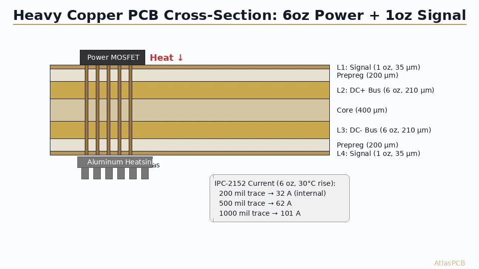
- Heavy Copper PCB Design for Power Electronics — High-current PCB alternatives
- PCB Copper Weight and Thickness Guide — Copper thickness selection for current capacity
- PCB Reflow Soldering Profile Optimization — Assembly considerations for MCPCB
Ready to design your next MCPCB? Get a quote from AtlasPCB — we manufacture aluminum and copper core PCBs from prototype through high-volume production with thermal conductivity options from 1.0 to 7.0 W/mK.
About AtlasPCB — We specialize in complex PCB manufacturing for HDI, RF, and high-reliability applications. Explore our heavy copper PCB manufacturing, or get an aluminum PCB manufacturing . Every order includes free engineering review. Get your quote.
Reviewed by AtlasPCB Engineering Team — IPC-certified manufacturing specialists with 15+ years of production experience in HDI, RF, and high-reliability PCB fabrication. Content based on factory floor data and real customer design reviews.
- MCPCB
- metal core PCB
- thermal management
- LED PCB
- power electronics
- aluminum PCB
- copper core
- IMS substrate