· AtlasPCB Engineering · Engineering · 15 min read
PCB Electrical Testing: Flying Probe vs Bed-of-Nails Fixture Testing Compared
A detailed comparison of flying probe and bed-of-nails fixture testing for PCB electrical verification. Understand when to use each method, their cost structures, test coverage differences, and how IPC-9252 defines net list testing requirements.
PCB Electrical Testing: Flying Probe vs Bed-of-Nails Fixture Testing Compared
A fabricated PCB is not a finished product until it has been electrically tested. No matter how well-controlled the etching, drilling, and plating processes are, defects happen — an under-etched trace creates a short between adjacent nets, a plating void in a through-hole creates an open circuit, a mis-registered drill breaks an inner-layer connection. These defects are invisible to visual inspection and AOI (automated optical inspection), which can only verify that the physical features look correct, not that they are electrically correct.
Electrical testing is the final gate that catches these defects before boards ship to the customer. The industry operates on a clear principle: 100% of boards must be electrically tested. Not a sample. Not a percentage. Every single board.
The two dominant methods — flying probe and bed-of-nails (BON) fixture testing — serve the same fundamental purpose but differ dramatically in speed, cost structure, flexibility, and test coverage. Choosing the right method for your order directly impacts cost, lead time, and the level of quality assurance you receive.
Why 100% Electrical Testing Is Non-Negotiable
Consider the economics. A bare PCB might cost $5–50 per unit. The components assembled onto it cost $50–5,000. The rework cost when an assembled board fails due to a bare-board defect is $100–1,000. The field failure cost — warranty claim, customer dissatisfaction, product recall — can reach $10,000 per unit or more.
Electrical testing catches defects at the lowest-cost stage of the value chain. A board that costs $20 to scrap before assembly would cost $2,000 to diagnose and rework after assembly. This is why IPC-9252 “Requirements for Electrical Testing of Unpopulated Printed Boards” establishes testing as a mandatory step, not an optional quality enhancement.
What Electrical Testing Catches
Opens (discontinuities): A net that should be continuous from point A to point B is broken. Causes include plating voids in through-holes, under-etched trace gaps, drill registration errors that miss inner-layer pads, and cracked traces from mechanical stress during processing.
Shorts (unintended connections): Two nets that should be isolated are electrically connected. Causes include under-etched copper bridges between traces, copper slivers from drilling or routing, plating deposits bridging between pads, and inner-layer shorts from mis-registration.
Isolation resistance failures: Nets are not fully shorted but have lower-than-acceptable isolation resistance between them. This can indicate contamination, hairline copper bridges, or dielectric degradation. These partial defects are particularly dangerous because they may pass a simple continuity test but fail in the field under voltage and temperature stress.
For a broader overview of PCB testing methods beyond electrical testing, see our guide on [PCB testing methods]/blog/pcb-testing-methods/).
Flying Probe Testing: Flexibility Without Fixtures
How It Works
A flying probe tester uses 2–8 motorized probe heads (typically 4: two on each side of the board) that move rapidly across the board surface, contacting individual test points in sequence to measure continuity and isolation. The test program is generated directly from the board’s netlist data — no physical fixture is required.
The test sequence follows the netlist:
Continuity test (opens): For each net, the probes contact two or more points on the net and measure resistance. A resistance below the threshold (typically 10–50 Ω, depending on trace length and copper weight) confirms the net is continuous. If the resistance exceeds the threshold, the net has an open.
Isolation test (shorts): The probes contact points on adjacent nets and measure isolation resistance. A resistance above the threshold (typically 2–10 MΩ) confirms the nets are isolated. If the resistance falls below, a short exists between the nets.
Modern flying probe systems achieve probe positioning accuracy of ±5–10 µm and can contact pads as small as 0.15 mm (6 mil) — smaller than most fixture pins can reliably hit. Probe heads move at speeds up to 60–100 measurements per second, depending on the system manufacturer (Takaya, ATG Luther & Maelzer, Seica, SPEA).
Advantages
Zero NRE cost. The test program is generated from Gerber/netlist data in software. There is no physical fixture to build, no fixture engineering charge, and no fixture lead time. For a one-off prototype, this means you pay nothing extra for electrical testing.
Instant design changes. If you revise your design, the test program updates in software. With fixture testing, a design change can mean scrapping a $2,000 fixture and building a new one.
Fine-pitch capability. Probe tips are smaller than fixture pins, allowing access to fine-pitch pads (0.15–0.3 mm) that would be impossible or unreliable with a bed-of-nails.
Double-sided probing. Most modern systems have probes on both the top and bottom, enabling testing of blind and buried vias that are only accessible from one side.
No minimum order sensitivity. Flying probe testing costs roughly the same per board whether you’re testing 1 board or 50 boards. There’s no fixture cost to amortize.
Limitations
Speed. This is the primary disadvantage. A moderately complex board (1,000 nets) takes 30–120 seconds per board on a 4-head flying probe system. A complex board (10,000+ nets) can take 5–15 minutes per board. For 10,000-unit production runs, this translates to 80–250 hours of test time — often impractical.
Limited simultaneous measurement. With only 4–8 probes, the system can test only one or a few nets at a time. Hi-pot (high-voltage isolation) testing between all possible net pairs would take impractically long, so flying probe systems typically test isolation only between adjacent nets — potentially missing shorts between non-adjacent nets routed in close proximity on different layers.
Probe mark cosmetics. The probe tips leave small indentation marks on pad surfaces. For most applications this is cosmetically acceptable, but for sensitive applications (gold bond pads, high-frequency pads where surface roughness affects performance), probe marks may be a concern. Modern systems minimize this with controlled probe force (typically 30–100 grams) and probe tip geometry optimization.
Bed-of-Nails Fixture Testing: Speed Through Parallelism
How It Works
A bed-of-nails (BON) test fixture is a custom-built array of spring-loaded pins (pogo pins) mounted in a precision-drilled plate. Each pin aligns with a specific test point on the board. When the board is placed on the fixture and compressed, all pins make simultaneous contact with all test points.
The test system then performs:
Continuity test: Current is driven through each net via its designated pins, and resistance is measured. All nets can be tested in rapid succession because all contact points are already connected.
Isolation test: Voltage is applied between net groups, and leakage current is measured. Hi-pot testing (typically 100–300V DC) can be applied between all adjacent net pairs simultaneously, providing thorough isolation verification.
Additional tests (optional): Some fixture-based systems can measure capacitance (to verify plane layers and embedded capacitors), resistance (to verify specific trace impedances), and even perform 4-wire Kelvin measurements for high-accuracy resistance verification.
Fixture Construction
A typical fixture consists of:
- Top plate: Precision-drilled acrylic or Delrin plate with holes positioned to match the board’s test points (accuracy ±0.05 mm)
- Pogo pins: Spring-loaded test probes, typically 100-mil or 75-mil center-to-center spacing, with tip diameters of 0.4–1.0 mm
- Wiring harness: Wires connecting each pin group to the test system’s measurement channels
- Base plate and pneumatic mechanism: Compresses the board against the pin array with controlled force
Fixture construction takes 3–7 business days and costs $500–5,000+ depending on board complexity (number of test points, board size, single-sided vs. double-sided).
Advantages
Speed. A fixture test completes in 3–10 seconds per board regardless of net count. A 10,000-net board tests in the same time as a 100-net board because all nets are accessed simultaneously. For high-volume production, this is decisive — 10,000 boards tested in 8–28 hours versus 80–250 hours for flying probe.
Comprehensive hi-pot testing. All net pairs can be subjected to high-voltage isolation testing simultaneously. This catches partial shorts and contamination-related isolation failures that low-voltage flying probe tests might miss.
Consistent contact. Every board is tested with the same pin positions, the same contact force, and the same measurement path. There’s no variability from probe positioning, which eliminates a potential source of false failures (or worse, false passes).
Additional measurement capability. Fixture-based systems can perform capacitance measurement (±10% accuracy) to verify that plane layers are correctly connected and that embedded passive components are within tolerance. This is beyond the capability of most flying probe systems.

Limitations
High NRE cost. The fixture must be custom-built for each unique board design. At $500–5,000+ per fixture, this is cost-prohibitive for prototypes or low-volume orders. A fixture for a complex double-sided board with 5,000+ test points can cost $3,000–5,000.
Fixture build lead time. 3–7 business days for fixture construction means you cannot use fixture testing for quick-turn prototype orders where 24–48 hour delivery is expected.
Design change sensitivity. Any change in test point location — moving a via, changing a pad size, adding a net — may require a new fixture or significant fixture modification. This is a hidden cost trap: ordering a production fixture before your design is frozen can result in scrapping a $3,000 fixture when a last-minute ECO changes a few vias.
Minimum pin pitch limitations. Standard pogo pins require 75–100 mil (1.9–2.5 mm) center-to-center spacing. Fine-pitch pins (50 mil / 1.27 mm) are available but more expensive and less reliable. For very fine-pitch boards (0.4 mm BGA pitch), there may not be enough accessible test points for complete fixture coverage without dedicated test pads.
Single-sided limitation. Most BON fixtures test from one side only (typically the bottom). Blind vias or pads accessible only from the top require either a double-sided fixture (significantly more expensive) or supplementary flying probe testing.
IPC-9252: The Standard for Electrical Testing
IPC-9252 “Requirements for Electrical Testing of Unpopulated Printed Boards” is the governing standard that defines what constitutes adequate electrical testing. Key requirements include:
Test Coverage
- All nets must be tested for both continuity and isolation. There is no acceptable partial testing — every net on the netlist must be verified.
- Test per approved netlist: The test program must be generated from the same netlist used for board fabrication. Any discrepancy between the fabrication data and the test data invalidates the test results.
Test Parameters
| Parameter | Typical Requirement |
|---|---|
| Continuity threshold (opens) | ≤50 Ω maximum resistance |
| Isolation threshold (shorts) | ≥2 MΩ minimum (standard), ≥10 MΩ (high-rel) |
| Test voltage (shorts) | 40–100 V DC (standard), up to 500 V (hi-pot) |
| Test voltage (opens) | 1–10 V DC |
Adjacency Testing
For isolation testing, IPC-9252 defines the concept of adjacency — which net pairs must be tested for shorts between them. At minimum, nets that are physically adjacent on any layer must be tested. Full adjacency testing (all possible net pairs) provides the most comprehensive coverage but dramatically increases test time for flying probe systems.
Fixture testing handles full adjacency efficiently because all nets are connected simultaneously — applying voltage between all possible pairs happens through the test system’s switching matrix in seconds.
Test Point Requirements
IPC-9252 doesn’t mandate specific test point sizes, but practical test point accessibility affects coverage:
- Flying probe minimum: 0.15 mm pad diameter, though 0.3 mm or larger is recommended for reliable contact
- Fixture pin minimum: 0.4 mm pad diameter for standard pins; 0.3 mm for fine-pitch pins
- Test point placement: Accessible from at least one board surface; not covered by soldermask (unless mask-over-pad testing is specified)
Cost Comparison: The Crossover Point
Understanding where flying probe and fixture testing costs cross over helps you make the right decision for each order:
Per-Board Cost Model
| Cost Component | Flying Probe | Fixture |
|---|---|---|
| NRE (one-time) | $0 | $500–5,000 |
| Programming | Included (auto from netlist) | Included |
| Per-board test cost | $1–5 (simple) / $5–20 (complex) | $0.10–0.50 |
| Test time per board | 30 sec – 15 min | 3–10 sec |
Crossover Analysis
For a moderately complex board ($2 flying probe per board, $1,500 fixture NRE, $0.25 fixture test per board):
- Break-even point: $1,500 / ($2.00 - $0.25) = 857 boards
- Below 857 boards: flying probe is cheaper
- Above 857 boards: fixture is cheaper
For a simple board ($1 flying probe, $500 fixture NRE, $0.10 fixture test):
- Break-even point: $500 / ($1.00 - $0.10) = 556 boards
For a complex board ($10 flying probe, $3,000 fixture NRE, $0.40 fixture test):
- Break-even point: $3,000 / ($10.00 - $0.40) = 313 boards
The pattern: more complex boards reach the fixture crossover sooner because the per-board flying probe cost increases with complexity while fixture per-board cost remains nearly constant.
When to Use Each Method
Use Flying Probe When:
- Prototype and NPI orders (<100-500 boards) where NRE isn’t justified
- Quick-turn orders where 3–7 day fixture build would delay delivery
- Designs in active revision where fixture investment is premature
- Very fine-pitch boards where fixture pin access is limited
- One-time builds with no expected repeat orders
Use Fixture Testing When:
- Production volumes (>500–1,000 boards per order or cumulative repeat orders)
- Design is frozen and no changes are expected
- High net-count boards where flying probe test time is impractical (>5 minutes per board)
- Hi-pot isolation testing is required (medical, automotive, aerospace)
- Capacitance or resistance measurements are needed for verification
- Repeat orders where the fixture investment is amortized across multiple production runs
Hybrid Approach
Many fabricators (including AtlasPCB) use a hybrid approach:
- Prototype phase: Flying probe testing (zero NRE, fast turnaround)
- Pilot production: Continue flying probe while fixture is built
- Volume production: Switch to fixture testing once the fixture is ready and design is stable
This approach minimizes both NRE risk (don’t build a fixture for an unproven design) and production cost (switch to fixture when volumes justify it).
For more on how testing differs between prototype and production phases, see our guide on [prototype vs production PCB manufacturing]/blog/pcb-prototype-vs-production/).
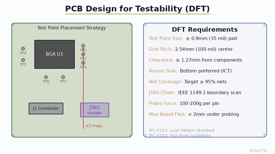
Design for Testability (DFT)
Regardless of which test method you’ll use, design choices affect test coverage and reliability:
Test Point Access
- Provide test pads on at least one surface for all nets. A net with no accessible pad on either surface cannot be tested by either method.
- Use 0.5 mm minimum pad diameter for test points when possible — reliable for both flying probe and fixture pins.
- Don’t cover test points with soldermask unless your fabricator confirms they can probe through mask openings.
Via-as-Test-Point
Open vias can serve as test points for flying probe testing (the probe contacts the annular ring or enters the hole). However, for fixture testing, vias are less reliable test points than flat pads because the pogo pin may not make consistent contact with the curved via surface.
Net Accessibility
Every net must have at least two accessible test points (one for each end of a continuity measurement). Single-point nets (e.g., a trace connecting only two pads, one of which is covered by a BGA) cannot be fully continuity-tested if only one point is accessible.
Separate Test Points from Component Pads
When possible, add dedicated test points separate from component pads. This ensures testability even when component pads are obstructed by nearby components during assembly verification.
Emerging Technologies
Combined Flying Probe + Vision Systems
Modern flying probe testers increasingly integrate optical inspection capabilities — cameras verify component markings, pad alignment, and surface quality alongside electrical testing. This combines AOI and electrical testing in a single machine pass, reducing total inspection time and cost.
Capacitance-Based Flying Probe Testing
Next-generation flying probe systems add capacitance measurement capability (traditionally a fixture-only feature). By measuring capacitance between a probe and the ground plane, these systems can detect inner-layer opens that resistance-only testing might miss — particularly useful for boards with large ground planes where an open trace still measures low resistance through capacitive coupling.
Contactless Testing
Research continues into fully contactless electrical testing using electromagnetic induction or capacitive coupling to verify connectivity without physical probe contact. While not yet commercially mainstream, these technologies promise to eliminate probe marks and enable testing of boards with no accessible test points — an increasingly common challenge as board density pushes toward test-point-free designs.
Reliability Testing Beyond Electrical Testing
Electrical testing verifies the board’s connectivity at time of manufacture. It does not verify long-term reliability. For applications demanding proven reliability, additional testing beyond bare-board electrical test is essential — including thermal shock testing, microsection analysis, and accelerated life testing. For more on these complementary approaches, see our guide on [PCB reliability testing]/blog/pcb-reliability-testing/).
Conclusion
Flying probe and bed-of-nails fixture testing are complementary tools, not competitors. Each has a clear domain where it excels:
- Flying probe is unbeatable for prototypes, low volumes, quick turns, and designs in flux — zero NRE, maximum flexibility, adequate speed for small quantities.
- Fixture testing is unbeatable for production volumes — fast, thorough, consistent, and cost-effective once the fixture investment is amortized.
The right choice depends on your order’s specific parameters: volume, lead time, design maturity, and test requirements. Most PCB engineers will use both methods across a product’s lifecycle — flying probe during development and fixture testing during production.
What matters above all is that every board is tested. The $1–5 per board cost of electrical testing is the cheapest insurance in electronics manufacturing.
Ready to start your project? Upload your Gerbers for a free engineering review, or talk to an engineer about your design requirements.
Further Reading
- [PCB Rigid-Flex Bend Zone Reliability: Design Rules, Material Selection & Lifecycle Testing]/blog/pcb-rigid-flex-bend-zone-reliability/)
- [ENEPIG vs ENIG Surface Finish: Complete Comparison for Wire Bonding, Solderability, and Long-Term Reliability]/blog/enepig-vs-enig-surface-finish-wire-bonding/)
- [PCB Surface Finish Comparison: OSP vs HASL vs Immersion Silver vs ENIG for Assembly Reliability]/blog/pcb-surface-finish-osp-hasl-enig-immersion-silver-comparison/)
- [Medical PCB Manufacturing: FDA Compliance, Traceability & Reliability]/blog/medical-pcb-manufacturing-requirements/)
- [Dynamic Flex PCB Design — Bend Radius, Material Selection, and Reliability]/blog/dynamic-flex-pcb-design-bend-radius-reliability/)
- Our Manufacturing Capabilities
About AtlasPCB — We specialize in complex PCB manufacturing for HDI, RF, and high-reliability applications. Explore our full PCB manufacturing capabilities . Every order includes free engineering review. Get your quote.
Reviewed by AtlasPCB Engineering Team — IPC-certified manufacturing specialists with 15+ years of production experience in HDI, RF, and high-reliability PCB fabrication. Content based on factory floor data and real customer design reviews.
- electrical-testing
- flying-probe
- fixture-testing
- quality-control
- ipc-9252