· AtlasPCB Engineering · Engineering · 7 min read
PCB Thermal Design for AI Inference Accelerators: Via Arrays, Copper Planes, and HDI Stackup Strategies
Engineering guide to PCB thermal management for AI inference hardware. Covers thermal via array design, copper plane allocation, HDI stackup optimization for 200-700W TDP AI chips, and material selection for sustained thermal cycling.
The Thermal Challenge: 700W Through a PCB
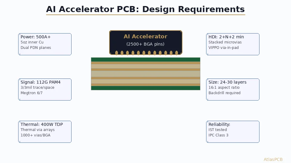
Modern AI inference accelerators (NVIDIA H100/H200, AMD MI300X, Intel Gaudi 3, custom ASICs) dissipate 300-700W in packages measuring 50-80mm per side. The PCB sits in the thermal path between the die and the heatsink/cold plate, and its thermal resistance directly impacts junction temperature.
Key numbers:
- Package thermal resistance (junction to case): 0.05-0.15 C/W
- PCB thermal resistance (case to heatsink mount): 0.5-3.0 C/W
- Heatsink/cold plate thermal resistance: 0.02-0.10 C/W
The PCB is often the worst thermal bottleneck in the stack. A poorly designed board adds 20-40C to junction temperature versus an optimized design.
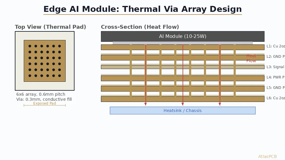
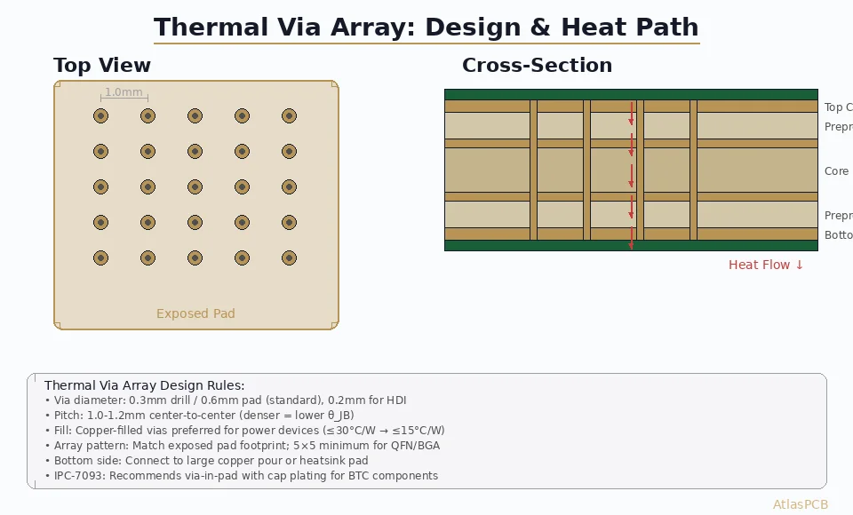
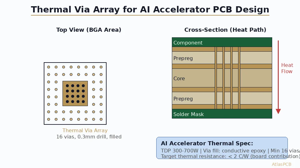
Thermal Via Array Design
Geometry Rules
The thermal via array under an AI chip’s exposed thermal pad is the primary vertical heat conduction path through the board:
| Parameter | Minimum Spec | Recommended | Notes |
|---|---|---|---|
| Via diameter | 0.25mm | 0.3mm | Larger = more copper fill area |
| Via pitch | 0.8mm | 0.6mm | Tighter pitch = more vias per area |
| Via fill | Conductive epoxy | Copper-filled | Copper fill 10x better than epoxy |
| Plating over fill | Required | Required | Enables SMT pad on top |
| Array size | 4x4 (16 vias) | 6x6 to 8x8 | Scale with TDP |
| Via depth | Through-board | Through-board | Blind thermal vias less effective |
Thermal Resistance Calculation
For a single filled thermal via (0.3mm drill, 25um wall plating, copper fill):
Via thermal conductivity: ~280 W/mK (copper fill) vs ~1.5 W/mK (epoxy fill)
Single via thermal resistance: R = L / (k * A)
- L = board thickness (1.6mm typical)
- A = via cross-section area (pi * 0.15^2 = 0.071 mm2)
- R_copper_filled = 1.6 / (280 * 0.071e-6) = ~80 C/W per via
16-via array: R_array = 80/16 = ~5 C/W (still significant!)
36-via array: R_array = 80/36 = ~2.2 C/W
64-via array: R_array = 80/64 = ~1.25 C/W
This shows why AI boards need 36-64 thermal vias — even copper-filled vias have meaningful resistance at PCB thicknesses.
Via Fill Options Compared
| Fill Type | Thermal Conductivity | Cost Premium | Reliability |
|---|---|---|---|
| Air (open via) | 0.025 W/mK | None | Poor (solder wicking) |
| Non-conductive epoxy | 0.5-1.0 W/mK | +10-15% | Good |
| Conductive epoxy (silver) | 3-8 W/mK | +20-30% | Good |
| Electroplated copper fill | 280 W/mK | +40-60% | Excellent |
For AI accelerator boards, conductive epoxy fill is the minimum. Copper-filled vias (VIPPO technology) are preferred for TDP above 400W.
AI HARDWARE PCB
Building AI Inference Hardware? We Optimize the Thermal Path
AtlasPCB fabricates up to 30-layer boards with copper-filled thermal via arrays, 5oz power planes, and High-Tg laminates for AI accelerator applications.
Submit AI Board Design ›Stackup Optimization for Thermal Performance
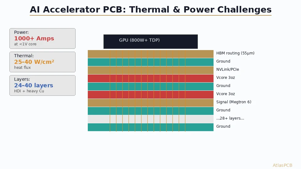
Layer Allocation Strategy
A typical 16-layer AI accelerator board allocates layers specifically for thermal management:
| Layer | Function | Copper Weight | Thermal Role |
|---|---|---|---|
| L1 | Component/Signal | 1oz | BGA pad thermal relief |
| L2 | Ground Plane | 2oz | Primary heat spreader |
| L3 | Signal | 0.5oz | Routing only |
| L4 | Power (VDD_CORE) | 2oz | Current + heat spreading |
| L5 | Signal | 0.5oz | Routing only |
| L6 | Ground Plane | 2oz | Thermal mass |
| L7 | Signal | 0.5oz | Routing only |
| L8 | Power (VDD_MEM) | 2oz | Current + heat spreading |
| … | … | … | … |
| L15 | Ground Plane | 2oz | Backside heat spreader |
| L16 | Component/Signal | 1oz | Backside thermal pad |
Design principles:
- Place ground planes adjacent to the component layer (L2 position) for immediate lateral heat spreading
- Use 2oz copper on all power/ground planes (doubles lateral thermal conductivity vs 1oz)
- Alternate signal and plane layers to maximize the number of copper planes in the stackup
- Bottom ground plane (L15 in this example) spreads heat to the backside cold plate
Material Selection for Sustained Thermal Cycling
AI inference boards operate at elevated temperatures continuously (not intermittent like consumer electronics). Material requirements:
| Property | Standard FR-4 | AI Board Requirement | Why It Matters |
|---|---|---|---|
| Glass transition (Tg) | 135-140C | 170C+ | Board near die reaches 100-130C |
| Decomposition temp (Td) | 300C | 340C+ | Prevents resin degradation over lifetime |
| Z-axis CTE (<Tg) | 50-60 ppm/C | <45 ppm/C | Reduces via barrel fatigue from cycling |
| Thermal conductivity | 0.3 W/mK | 0.4-0.5 W/mK | Higher = better lateral spreading |
| CAF resistance | Standard | Enhanced | High voltage + humidity near hot zones |
Recommended laminates for AI server boards:
- Isola 370HR (Tg 180C, Td 350C) — proven in hyperscale data centers
- Panasonic Megtron 6 (Tg 175C, low Dk/Df) — when signal integrity also critical
- Nelco N7000-2 HT (Tg 200C) — extreme temperature applications
Copper Plane Heat Spreading Effectiveness
A solid 2oz copper plane spreads heat laterally with this characteristic:
- Spreading radius for 10C temperature drop: ~25mm from heat source center
- A 50mm BGA on a solid 2oz plane achieves 60-70% of theoretical infinite plane spreading
- Plane splits for different voltage domains reduce spreading — keep thermal ground plane continuous
Critical rule: Never split the ground plane directly under a high-TDP component. Route power domains on other layers and keep the primary ground plane (L2) as a continuous thermal spreader.
HDI CAPABILITIES
Up to 30 Layers with Controlled Impedance and Heavy Copper
HDI stackups with 5+N+5 buildup, stacked microvias, and 2oz inner planes. Optimized for high-pin-count AI processors.
Common Failure Modes and Prevention
1. Via Barrel Cracking from Thermal Cycling
AI boards cycle between idle (30-40C) and full inference load (100-130C near die) hundreds of thousands of times over their 5-7 year data center lifetime. Each cycle stresses via barrels through Z-axis CTE mismatch.
Prevention:
- Use low-CTE laminate (<45 ppm/C in Z-axis)
- Specify minimum 25um copper plating thickness in via barrels
- Avoid aspect ratios above 10:1 for through-board vias
- Consider back-drilled vias to reduce barrel length for non-thermal vias
AtlasPCB supports aspect ratios up to 16:1 with enhanced plating processes for boards up to 5.5mm thick.
2. Solder Joint Fatigue Under Thermal Gradient
Large BGAs on AI chips experience significant temperature gradients — the center pad may be 20-30C hotter than corner pads during operation. This differential thermal expansion causes accelerated solder fatigue at the package corners.
Prevention:
- Uniform thermal via distribution (not just center — extend to outer pad rows)
- CTE-matched underfill on critical packages
- Design for controlled die tilt: symmetrical stackup to prevent board warpage
3. Delamination Near Hot Zones
Sustained temperatures above 0.8 x Tg cause moisture-driven delamination in standard FR-4. Near AI chips:
- Board temperature reaches 100-130C continuously
- Standard Tg 135C FR-4 is operating above 0.8 x Tg (108C)
- Moisture trapped during lamination outgases and causes blistering
Prevention:
- High-Tg laminate (Tg 170C+) ensures operation well below 0.8 x Tg
- Pre-bake boards before assembly (125C, 4 hours minimum)
- Specify moisture-sensitive packaging for bare boards stored before assembly
4. CAF (Conductive Anodic Filament) Growth
High voltage differentials (12V, 48V power rails on AI server boards) combined with elevated temperature and humidity create conditions for CAF growth between closely-spaced vias or between via and trace.
Prevention:
- Minimum 0.4mm via-to-via spacing on different nets with >25V differential
- Use CAF-resistant laminate (enhanced resin systems with filler particles)
- Avoid drilling through glass bundles (use drill-to-copper clearance >8mil)
RELIABILITY TESTING
Thermal Cycling Qualification for AI Server Boards
IST, thermal shock, and microsection analysis to validate via reliability before volume production. IPC Class 3 inspection standard.
Discuss Your Project ›Design Checklist for AI Inference PCBs
Before sending your AI accelerator board design to fabrication:
- Thermal via array: minimum 36 vias per thermal pad, 0.3mm drill, filled
- Ground plane (L2) continuous under all high-TDP devices — no splits
- 2oz minimum on all power/ground planes
- High-Tg laminate specified (Isola 370HR, Megtron 6, or equivalent)
- Via aspect ratio under 12:1 (under 10:1 preferred)
- Copper fill percentage balanced within 15% between paired layers
- Back-drilling specified for signal vias in high-speed memory interface regions
- Power delivery network: adequate decoupling via count and placement
- Thermal simulation completed (ANSYS Icepak, 6SigmaET, or equivalent)
- Board thickness appropriate for cold plate mounting flatness requirement
ATLASPCB
AI Hardware PCB Fabrication: From Prototype to Volume
Copper-filled vias, 30-layer HDI, controlled impedance, High-Tg materials. Purpose-built for AI accelerator thermal and signal integrity demands.
Get Instant Quote ›Related Reading:
About AtlasPCB — We specialize in complex PCB manufacturing for HDI, RF, and high-reliability applications. Explore our HDI PCB manufacturing capabilities, or get an aluminum and metal-core PCB services . Every order includes free engineering review. Get your quote.
Reviewed by AtlasPCB Engineering Team — IPC-certified manufacturing specialists with 15+ years of production experience in HDI, RF, and high-reliability PCB fabrication. Content based on factory floor data and real customer design reviews.
- AI hardware
- thermal management
- PCB design
- thermal via
- HDI
- data center
- inference accelerator