· AtlasPCB Engineering · Engineering · 8 min read
PCB Design for Testability (DFT): Test Point Placement, ICT Access, and Boundary Scan Strategy
Complete guide to PCB design for testability. Learn IPC-9252 test point requirements, bed-of-nails fixture access rules, flying probe accommodation, JTAG boundary scan integration, and how DFT reduces manufacturing defect escape rates below 10 ppm.
Why Design for Testability Matters in PCB Manufacturing
Every PCB that leaves a production line must pass electrical verification. Without deliberate testability design, you face two expensive outcomes: either defective boards escape to the field (costing 10-100× more to fix), or your test coverage is so low that false passes undermine quality metrics.
Design for Testability (DFT) is the practice of embedding testability features — accessible test points, JTAG chains, power rail isolation — into your PCB layout from the start. It costs almost nothing in board area (typically 2-4% area overhead) but saves thousands in fixture redesigns, test programming time, and field returns.
This guide covers the complete DFT methodology, from test point sizing per IPC-9252 to boundary scan chain planning per IEEE 1149.1, with practical layout rules that work across bed-of-nails ICT, flying probe, and functional test platforms.
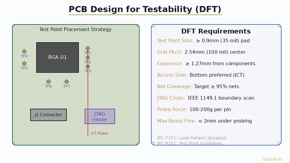
Test Point Fundamentals: Size, Grid, and Placement
IPC-9252A Test Point Requirements
The IPC-9252A standard defines test point requirements for board-level electrical testing:
| Parameter | Minimum | Recommended |
|---|---|---|
| Pad diameter | 0.9 mm (35 mil) | 1.0 mm (40 mil) |
| Center-to-center pitch | 1.27 mm (50 mil) | 2.54 mm (100 mil) |
| Clearance from components | 1.0 mm | 1.27 mm |
| Clearance from board edge | 2.5 mm | 3.0 mm |
| Pad height (from surface) | Flat (flush) | < 0.5 mm protrusion |
Test Point Placement Strategy
Bottom-side priority: Place all test points on the PCB’s bottom (secondary) side. This allows a standard bed-of-nails fixture to access all points simultaneously while components sit on the top side undisturbed.
Net coverage target: Aim for ≥95% net accessibility. Every signal net, power rail, and ground connection should have at least one test point. The 5% allowance covers nets that physically cannot route to an accessible pad (e.g., BGA inner balls on via-in-pad).
Grid alignment: Align test points to a 2.54mm (100 mil) grid when possible. Fixture drill plates use standard grid patterns, and grid-aligned points reduce fixture cost by $200-800 per design.
Keep-out zones: Maintain 5mm minimum clearance from fixture tooling holes (registration pins) and 3mm from board edges where clamp mechanisms operate.
Test Point Types
- Dedicated test pads — standalone pads connected to the target net via short traces. Most reliable for probe contact.
- Via test points — exposed vias (tented on top, open on bottom) serving dual purpose as routing vias and test access. Acceptable but less reliable than flat pads.
- Component pad access — using existing component pads (e.g., resistor pads, connector pins) as test points. Works for through-hole components; risky for fine-pitch SMD.
In-Circuit Test (ICT) Design Guidelines
Bed-of-Nails Fixture Requirements
A bed-of-nails fixture uses spring-loaded probes (pogo pins) pressed against test points to verify electrical connectivity. Key design considerations:
Probe force budget: Each probe exerts 100-200 grams of force. A board with 1,000 test points experiences 100-200 kg total force. Ensure your PCB thickness and support structure can handle this without excessive deflection (< 2mm).
Probe types and sizes:
- Standard probe: 1.0mm tip for 0.9mm+ pads
- Fine-pitch probe: 0.5mm tip for 0.6mm pads (expensive, less durable)
- Crown probe: serrated tip for penetrating oxide layers on OSP/HASL finishes
Board support: Design tooling hole locations (minimum 2, prefer 4 corners) for fixture registration. Use 3.2mm diameter unplated holes at known coordinates, documented in your fabrication drawing.
Net Isolation for Component Testing
ICT can measure individual component values (resistance, capacitance, semiconductor junctions) by isolating nets. Enable this by:
- Isolation capacitors: Add 0Ω resistor positions in series with power rails to allow test-mode isolation
- Power sectioning: Design test points on both sides of voltage regulators for input/output measurement
- Guard points: Place test points on adjacent nets to enable guarding (driving known voltages to prevent parallel paths from affecting measurements)

Need DFT-Optimized PCB Manufacturing?
AtlasPCB provides free DFM/DFT review with every order. Our engineers verify test point accessibility before production.
Get a Free DFT Review →Flying Probe Test Accommodation
Not every board goes through bed-of-nails ICT. Prototypes, low-volume builds, and boards with frequent revisions use flying probe testing instead.
Flying Probe Access Requirements
Flying probe testers use 4-8 movable probes that sequentially contact test points. Design considerations differ from ICT:
- Access from both sides: Flying probes can reach top and bottom, so dual-side test points are acceptable
- Clearance from tall components: Probes approach vertically — ensure 2mm height clearance above each test point (no tall capacitors directly over bottom-side pads)
- Sequential vs. parallel: Test time scales linearly with net count (30 seconds to 5+ minutes per board), so minimize unnecessary test points on low-risk nets
- No fixture grid requirement: Points need not align to a grid, giving more layout freedom
Hybrid Strategy: Design for Both
The optimal approach designs for bed-of-nails ICT (bottom-side grid) while ensuring flying probe access for engineering validation:
- Place primary test points on bottom side (2.54mm grid) for ICT
- Add supplementary top-side points on critical signals for flying probe debug
- Document both test point lists in your test access documentation
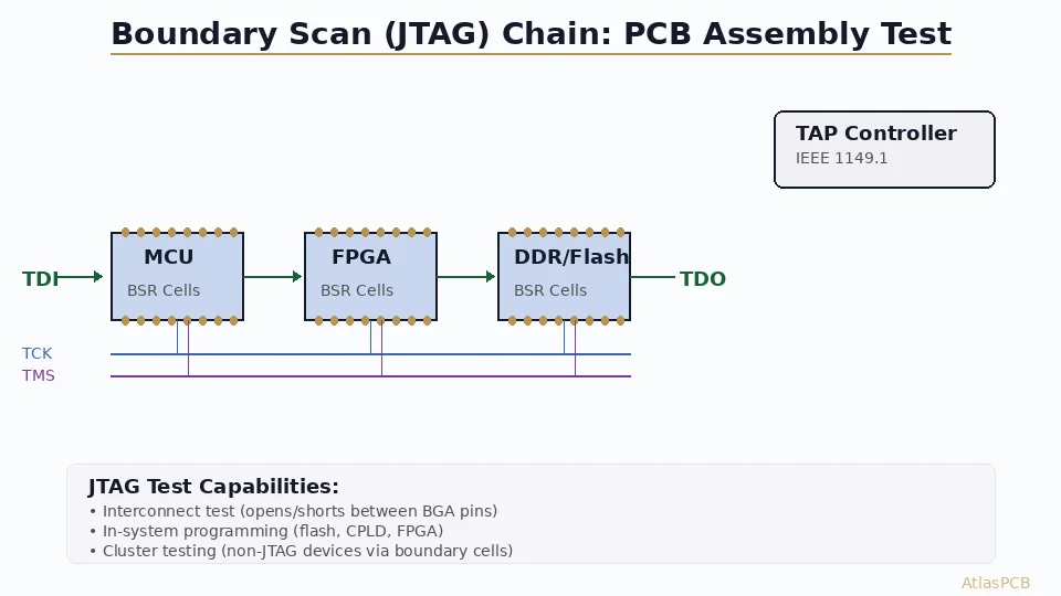
Boundary Scan (JTAG) Integration
IEEE 1149.1 Boundary Scan Architecture
For digital-heavy designs, boundary scan testing through the JTAG chain provides coverage that physical probing cannot reach — particularly BGA inner balls and fine-pitch connections.
JTAG chain requirements:
- TDI, TDO, TCK, TMS, and optional TRST signals must be accessible
- Dedicate a test header (2x5 or 2x7 pin) with 2.54mm pitch
- Route JTAG signals with controlled impedance if chain operates above 10 MHz
- Include series resistors (33Ω) on TCK and TMS for signal integrity
Chain topology planning:
- Connect all boundary-scan-capable ICs in a single chain (TDO of IC1 → TDI of IC2)
- Place FPGAs and processors at the start of the chain (most likely to be tested)
- Include bypass capacitors on TCK at each device
- Add test points on TDI/TDO between ICs for chain segment isolation during debug
What Boundary Scan Tests
| Test Type | Coverage | Detection |
|---|---|---|
| Infrastructure | JTAG chain connectivity | Stuck-at faults on JTAG signals |
| Interconnect | Pin-to-pin connections | Opens and shorts between ICs |
| Memory BIST | Embedded RAM blocks | Memory cell failures |
| I/O toggle | Output driver functionality | Driver failures, stuck outputs |
Combining ICT and Boundary Scan
The highest fault coverage comes from combining physical probe access with boundary scan:
- ICT tests passive components, power rails, and analog circuits
- Boundary scan tests digital interconnections, especially BGA-to-BGA links
- Together they achieve >99% structural fault coverage
Test Coverage Metrics and Targets
Defect Coverage Hierarchy
| Test Method | Typical Coverage | Defect Escape Rate |
|---|---|---|
| Visual inspection only | 40-60% | 500+ ppm |
| AOI + visual | 70-80% | 200-300 ppm |
| Flying probe (nets only) | 85-92% | 50-100 ppm |
| ICT (full access) | 95-98% | 10-30 ppm |
| ICT + boundary scan | 98-99.5% | 2-10 ppm |
| ICT + boundary scan + FVT | 99.5-99.9% | < 5 ppm |
Calculating Test Access Percentage
Test access percentage = (Accessible nets / Total nets) × 100%
For IPC Class 3 (high-reliability) applications, target ≥98% test access. For commercial products, ≥90% is acceptable.
Common access blockers:
- BGA inner ball rows without via-in-pad test access
- Bottom-side components blocking probe access to pads beneath them
- Insufficient board-edge clearance for fixture clamps
- Component height blocking probe approach angle
DFT Checklist for PCB Designers
Use this checklist during layout review:
Test Point Design:
- All signal nets have at least one test point
- Test point pads ≥ 0.9mm diameter
- Minimum 1.27mm center-to-center spacing
- Bottom-side placement preferred for ICT
- 3mm clearance from board edges
- No tall components directly above bottom-side test points
Fixture Compatibility:
- Registration/tooling holes placed (2-4 per board)
- Test point coordinates documented in pick-and-place data
- Board thickness supports probe force (1.6mm+ recommended)
- Panel design allows fixture access (no rails over test points)
Boundary Scan:
- JTAG header accessible at board edge
- Chain order documented in schematic
- Series resistors on TCK/TMS
- TRST has pull-up or pull-down to prevent unintended resets
Documentation:
- Test point list exported with X/Y coordinates and net names
- Test access percentage calculated and documented
- Non-accessible nets listed with justification
Common DFT Mistakes and How to Avoid Them
Mistake 1: Adding Test Points After Layout
DFT must be part of the initial layout constraint setup, not an afterthought. Adding test points post-routing often means poor routing to reach accessible locations, increased board area, and compromised signal integrity.
Solution: Define test point zones in your PCB template before component placement. Reserve bottom-side regions for test point routing.
Mistake 2: Using Via Test Points with Solder Mask
If vias serving as test points are tented with solder mask, probes cannot make contact. Ensure test vias are mask-open on the access side.
Solution: Add “test” attribute to vias in your EDA tool and configure mask opening rules accordingly.
Mistake 3: Ignoring Probe Approach Angle
Fixture probes approach at exactly 90° to the board surface. Any component taller than 5mm within 1.5mm of a test point can physically block the probe.
Solution: Create a 3D clearance check in your DFM/DFT verification step. Many EDA tools support probe clearance DRC rules.
Further Reading
- PCB Electrical Testing: Flying Probe vs Bed-of-Nails Fixture — Detailed comparison of the two primary test methods
- Boundary Scan JTAG Testing: IEEE 1149.1 Guide — Deep dive into boundary scan architecture
- IPC-A-610 Class 3 Inspection and Workmanship — Quality acceptance criteria for high-reliability PCBs
- BGA X-Ray Void Analysis per IPC-7095 — Inspection techniques for hidden solder joints
Need PCBs manufactured with testability in mind? AtlasPCB’s engineering team reviews every design for DFT compliance before production. We flag inaccessible nets, suggest test point additions, and ensure your boards are ready for ICT or flying probe testing from day one. Request a free DFT review →
About AtlasPCB — We specialize in complex PCB manufacturing for HDI, RF, and high-reliability applications. Explore our full PCB manufacturing capabilities . Every order includes free engineering review. Get your quote.
Reviewed by AtlasPCB Engineering Team — IPC-certified manufacturing specialists with 15+ years of production experience in HDI, RF, and high-reliability PCB fabrication. Content based on factory floor data and real customer design reviews.
- design-for-testability
- test-points
- ict-testing
- boundary-scan
- ipc-9252
- dft
- quality-control