· AtlasPCB Engineering · Engineering · 7 min read
PCB Requirements for AI Accelerator Hardware: Layer Count, Power Delivery, and Thermal Design
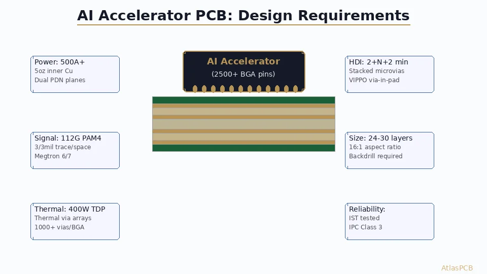
Designing PCBs for AI accelerators (GPUs, TPUs, custom ASICs) demands extreme specifications: 20-30 layers, 500A+ current delivery, 3/3mil routing, and advanced thermal management. Here's what your fabricator needs to deliver.
The Most Demanding PCBs in Commercial Electronics
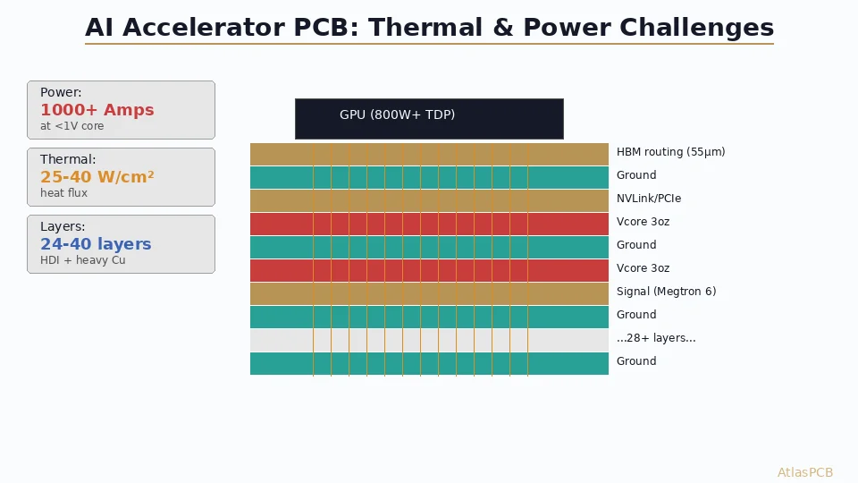
AI accelerator hardware represents the convergence of every challenging PCB specification simultaneously: high layer count, HDI microvia structures, heavy copper power delivery, ultra-low-loss materials, extreme thermal management, and tight impedance control. A single AI training card can cost $3,000-10,000 just for the bare PCB—before any components.
This guide covers what it takes to fabricate these boards and how design choices impact manufacturability and cost.
Layer Count: Why 20-30 Layers is the Minimum
The Driving Forces
A modern AI accelerator (Nvidia B200, AMD MI300X, Google TPU v5) connects to:
- HBM3e memory: 8-12 stacks, each with 1024+ I/O at 9.6 Gbps
- PCIe Gen6 or NVLink: 112G PAM4 per lane, 16-72 lanes
- Power delivery: 0.7-0.85V core at 500-1000A
- Management/control: I2C, SPI, GPIO, thermal sensors
Routing all of this requires:
| Layer Type | Count | Purpose |
|---|---|---|
| Signal (high-speed) | 8-12 | HBM, PCIe, NVLink traces |
| Signal (low-speed) | 2-4 | Control, I2C, GPIO |
| Ground reference | 6-8 | Adjacent to every signal layer |
| Power planes | 4-8 | Multiple voltage rails at high current |
| Total | 20-30 | Typical range |
Why Not Fewer Layers?
Every signal layer needs an adjacent ground reference plane for impedance control. That alone means signal + reference = 2 layers per routing tier. With 6-8 routing tiers needed for BGA escape and interconnect, plus 4-8 power planes for current density, you quickly reach 20+ layers.
Reducing layer count means wider boards (more routing space needed) or higher-density HDI (more expensive buildup). At AI-scale pin counts, 20-30 layers is actually the cost-optimized solution.
HIGH LAYER COUNT
Up to 30-Layer PCBs for AI and HPC Applications
AtlasPCB fabricates 20-30 layer boards with HDI buildup, Megtron 6 laminates, and 5oz copper power planes for AI hardware.
Get Quote for AI Board ›Power Delivery: 500A+ at Sub-1V
The Challenge
Modern AI accelerators draw 500-1000A at 0.7-0.85V. At these currents, even milliohms of PDN impedance create unacceptable voltage droop. The PCB power delivery network must achieve:
- DC resistance: < 0.5 milliohm from VRM to BGA
- AC impedance: < 1 milliohm up to 100 MHz
- Current capacity: 500A sustained, 800A+ transient
Copper Weight Requirements
Standard 1oz (35um) copper on a 50mm-wide power plane carries approximately 30A with acceptable temperature rise. To deliver 500A, you need:
| Copper Weight | Current per 50mm Width | Planes Needed (500A) |
|---|---|---|
| 1oz (35um) | ~30A | 17 planes (impossible) |
| 2oz (70um) | ~60A | 9 planes |
| 3oz (105um) | ~90A | 6 planes |
| 5oz (175um) | ~150A | 4 planes |
Practical designs use 3-5oz copper on 4-6 power/ground plane pairs, supplemented by wide copper pours on signal layers.
Via Current Distribution
The BGA-to-plane connection uses massive via arrays. A typical AI accelerator BGA has:
- 300-500 power pins
- 300-500 ground pins
- Each via carries 1-2A average
Via resistance dominates at these currents. For a 0.3mm via in a 3.5mm board:
- 0.5oz plating: ~6 milliohm per via
- 1.0oz plating: ~3 milliohm per via
1000 vias in parallel: 3-6 microhm contribution — acceptable.
Signal Integrity: 112G PAM4 on a PCB
Material Requirements
112G PAM4 signaling (the Nyquist frequency is ~28 GHz for 56 Gbaud) demands:
| Parameter | Requirement | Standard FR-4 | Megtron 6 | Megtron 7 |
|---|---|---|---|---|
| Df @ 12.5 GHz | < 0.004 | 0.020 | 0.002 | 0.001 |
| Dk variation | < +/-3% | +/-5% | +/-2% | +/-1.5% |
| Surface roughness | < 2um Rz | 6-8um | 2-3um (VLP) | 1-2um (HVLP) |
| Insertion loss (6”) | < 8 dB @ 28 GHz | >20 dB | 5-6 dB | 3-4 dB |
The copper surface roughness contribution to loss becomes dominant above 10 GHz. HVLP (Hyper Very Low Profile) copper is mandatory — standard RTF (Reversed Treat Foil) adds 3-4 dB/inch at 28 GHz.
Backdrilling: Eliminating Via Stubs
A through-via in a 24-layer board creates a stub from the signal exit point to the via end. At 28 GHz, even a 0.5mm stub creates destructive resonance. Backdrilling removes the unused stub portion:
- Target stub length: < 0.2mm (200um)
- Backdrilling accuracy: +/-3mil (AtlasPCB specification)
- Required on: all high-speed signal vias not on outer layers
Without backdrilling, via stubs create notch filters that kill eye diagrams above 16 GHz.
SIGNAL INTEGRITY
Low-Loss Materials + Precision Backdrilling
Megtron 6/7 laminates with HVLP copper foil and backdrilling to +/-3mil stub accuracy for 56+ Gbaud signaling.
View Signal Integrity Specs ›Thermal Management: Conducting Heat Through the PCB
Thermal Via Arrays
With 400W+ TDP concentrated in a 50x50mm die area, the PCB beneath becomes a thermal bottleneck. Thermal via arrays provide vertical heat conduction:
| Via Configuration | Thermal Conductivity (W/mK) | Typical Application |
|---|---|---|
| No thermal vias | 0.3 (FR-4 only) | Not acceptable |
| Via array (0.3mm, 1mm pitch) | 3-8 | Moderate power |
| Dense via array (0.2mm, 0.5mm pitch) | 15-25 | High power |
| Filled via array (copper-filled) | 30-50 | AI accelerator |
For AI boards, the area directly under the chip (die shadow) contains 1000-2000 copper-filled thermal vias in a tight grid, connected to internal copper planes that spread heat laterally to board edges and mounting hardware.
Heavy Copper as Heat Spreader
Internal 3-5oz copper planes serve dual duty: power delivery AND thermal spreading. A 5oz (175um) copper plane has thermal conductivity of 400 W/mK along its plane — 1300x better than FR-4. This makes the internal planes the primary lateral heat transport mechanism.
Manufacturing Challenges and Yield
Aspect Ratio
24-layer board, 3.5mm thickness, 0.2mm via drill: aspect ratio = 17.5:1
This exceeds standard capability. Solutions:
- Use 0.25mm minimum drill (14:1 aspect ratio) — acceptable
- Backdrilling reduces effective depth
- HDI structure avoids full-depth through-vias for many connections
Registration
At 24+ layers, layer-to-layer registration stacking becomes critical. Each layer adds +/-25um registration error. After 24 layers, total stack can reach +/-75-100um, eating into annular ring budgets.
Solution: fabricators use sequential alignment (re-registering every 4-6 layers) rather than single-stack alignment.
Yield Impact
| Board Type | Typical First-Pass Yield |
|---|---|
| 8-layer standard | 95-98% |
| 16-layer HDI | 88-93% |
| 24-layer AI (standard materials) | 80-88% |
| 24-layer AI (Megtron 6, backdrill) | 75-85% |
| 30-layer ELIC + Megtron 7 | 65-78% |
Lower yield directly impacts cost — and why AI PCBs carry premium pricing.
AI HARDWARE FABRICATION
High-Complexity PCBs for AI Infrastructure
Up to 30 layers, 5oz copper, 16:1 aspect ratio, Megtron 6. We manufacture the boards that power AI data centers.
Explore HDI Services ›Specification Summary for AI Accelerator PCBs
| Parameter | Typical Requirement | AtlasPCB Capability |
|---|---|---|
| Layer count | 20-30 | Up to 30 |
| HDI structure | 2+N+2 to 4+N+4 | Up to 5+N+5 |
| Trace/space | 3/3mil (75um) | 3/3mil minimum |
| Copper weight (inner) | 2-3oz | Up to 3oz |
| Copper weight (outer) | 2-5oz | Up to 5oz |
| Min laser drill | 0.075mm | 0.075mm |
| Aspect ratio | 14-16:1 | Up to 16:1 |
| Material | Megtron 6/7 | Megtron 6 available |
| Backdrilling | +/-3mil stub | +/-3mil accuracy |
| Board size | 300x300mm+ | Up to 1200x600mm |
| Surface finish | ENIG | ENIG, immersion silver |
| Impedance tolerance | +/-5% | +/-5% with TDR coupon |
ATLASPCB
Building AI Hardware? Let's Talk Specifications.
Upload your stackup or design files. Our engineering team has experience with high-layer-count AI boards and can provide detailed DFM feedback within 48 hours.
Upload Design Files ›Related Reading:
- Advanced HDI PCB Stackup Design: Sequential Lamination, Any-Layer HDI, and ELIC
- High Layer Count PCB Challenges: Designing and Manufacturing 20 to 68 Layer Boards
- Signal Integrity in PCB Design: Impedance Control, Crosstalk, Via Stubs, and Return Paths
- PCB Thermal Via Design: Complete Engineering Guide
About AtlasPCB — We specialize in complex PCB manufacturing for HDI, RF, and high-reliability applications. Explore our HDI PCB manufacturing capabilities, or get an aluminum and metal-core PCB services . Every order includes free engineering review. Get your quote.
Reviewed by AtlasPCB Engineering Team — IPC-certified manufacturing specialists with 15+ years of production experience in HDI, RF, and high-reliability PCB fabrication. Content based on factory floor data and real customer design reviews.
- AI hardware
- PCB design
- GPU
- accelerator
- HDI
- power delivery
- thermal management
- high layer count