· AtlasPCB Engineering · Engineering · 8 min read
PCB Heatsink Attachment Methods: Thermal Adhesive, Mechanical Clip, and Solder Reflow Mounting
Compare PCB heatsink attachment methods including thermal adhesive, spring-clip mechanical mounting, and solder-reflow bonding. Learn thermal resistance values, rework considerations, and design rules for each approach to optimize power dissipation in high-current PCB assemblies.
The Thermal Challenge in Modern PCB Design
Modern power electronics push component thermal design power (TDP) from 5W for simple voltage regulators to 150W+ for high-performance processors and GaN power stages. The heatsink attachment method directly determines whether that heat reaches the ambient effectively or accumulates until thermal shutdown.
Choosing the wrong attachment method leads to either premature field failures (adhesive degradation in thermal cycling), unnecessary board complexity (mechanical mounting holes consuming routing space), or impossible rework scenarios. This guide provides the engineering data to make the right choice for your power level, reliability class, and production constraints.
Thermal Interface Fundamentals
The Thermal Resistance Stack
The total thermal resistance from junction to ambient follows a series path:
Tj → Rjc → Rcs → Rsa → Ta

Where:
Tj  = Junction temperature
Rjc = Junction-to-case (IC package dependent)
Rcs = Case-to-sink (YOUR attachment method)
Rsa = Sink-to-ambient (heatsink design)
Ta  = Ambient temperature
The case-to-sink interface (Rcs) is what your attachment method controls. It ranges from 0.2°C/W (soldered interface) to 5°C/W (poor adhesive application with air gaps).
Why Attachment Method Matters More Than Heatsink Size
A common design mistake: specifying a larger, more expensive heatsink to compensate for a poor thermal interface. The math shows why this fails:
Example: IC with TDP = 20W, Rjc = 1.0°C/W, required Tj < 100°C, Ta = 40°C
- Budget: Rcs + Rsa < (100 - 40)/20 - 1.0 = 2.0°C/W total
- With good adhesive (Rcs = 2.0°C/W): Need Rsa < 0°C/W — impossible!
- With solder reflow (Rcs = 0.3°C/W): Need Rsa < 1.7°C/W — achievable with a modest 30×30×10mm heatsink
The interface thermal resistance often dominates the entire thermal path.
Method 1: Thermal Adhesive Attachment
Types of Thermal Adhesives
Thermal epoxy (2-part):
- Thermal conductivity: 1.0-3.0 W/m·K
- Bond strength: 50-200 psi
- Typical Rcs: 1.5-3.0°C/W (depends on bondline thickness)
- Cure time: 4-24 hours at room temperature, or 1 hour at 80°C
- Examples: 3M TC-2810, Arctic Silver Thermal Adhesive, Masterbond EP21TCHT-1
Thermal tape (pressure-sensitive):
- Thermal conductivity: 0.6-1.5 W/m·K
- Bond strength: 20-80 psi
- Typical Rcs: 2.0-4.0°C/W
- Instant bond, no cure time
- Examples: 3M 8810, Bergquist Gap Pad, Laird Tflex
Thermal grease + mechanical retention:
- Thermal conductivity: 3.0-12.0 W/m·K (highest)
- Bond strength: None (requires separate retention)
- Typical Rcs: 0.2-0.8°C/W
- Must be combined with clips or screws
- Examples: Shin-Etsu X-23-7783D, Thermal Grizzly Kryonaut
Design Rules for Adhesive Attachment
Pad preparation: The PCB copper pad under the heatsink must be exposed (solder mask opening) and flat. ENIG or HASL finish provides good adhesive bonding; OSP requires adhesion promoter.
Bondline thickness: Control adhesive thickness to 50-100μm for optimal thermal performance. Thicker bondlines (>200μm) dramatically increase Rcs.
Coverage area: Apply adhesive to cover ≥80% of the interface area. Voids and air pockets create thermal hot spots.
Cure profile: For thermal epoxy, follow manufacturer cure schedule exactly. Under-cured adhesive has higher Rcs and lower long-term reliability.
CTE matching: Select adhesives with CTE (coefficient of thermal expansion) between the heatsink material (aluminum: 23 ppm/°C) and PCB (FR-4: 14-17 ppm/°C in-plane). Mismatched CTE causes adhesive fatigue in thermal cycling.
When to Use Thermal Adhesive
- Power dissipation < 10W
- No rework requirement
- Space-constrained designs (no room for mounting hardware)
- Cost-sensitive applications (no additional fasteners)
- Low vibration environments
Method 2: Mechanical Clip and Push-Pin Mounting
Clip Mechanism Types
Spring clips (Z-clip): Metal spring clips hook under the PCB edge or through board holes to press the heatsink against the component. Provides consistent pressure (typically 2-5 lbs force) regardless of thermal cycling.
Push-pin (Aavid/Boyd style): Plastic or metal pins insert through board holes and lock with expanding tips. Simple assembly but limited force control and potential for pin fatigue.
Screw-down with standoffs: Threaded standoffs bonded or pressed into the PCB provide the most controlled mounting force. Used in high-reliability applications (telecom, server).
Board-level clamp: PCB-mounted retention brackets that capture the heatsink from the sides. Common for TO-220 and TO-247 power packages.
Design Rules for Mechanical Mounting
Mounting hole placement: Position holes symmetrically around the thermal interface center. Uneven hole placement creates tilting and non-uniform pressure.
Hole diameter:
- Push-pin: 3.0-3.2mm through-hole (unplated)
- Screw: 2.7-3.3mm (M3 clearance) with plated barrel for ground connection
- Spring clip: Slot or hole per clip manufacturer specification
Keep-out on inner layers: Mounting holes interrupt copper planes. Route power/ground planes around holes with 0.5mm clearance. Add stitching vias around holes to maintain ground plane continuity.
Board flex analysis: Calculate board deflection under probe/clip force:
- FR-4 Young’s modulus: ~20 GPa
- 1.6mm board, 40mm span, 5 lb center load → ~0.3mm deflection (acceptable)
- 0.8mm board, same conditions → ~2.4mm deflection (excessive — add stiffener)
Thermal interface material (TIM): Mechanical mounting always requires a TIM between heatsink and component. Use thermal pads (0.5-2.0mm thick) or grease. Never rely on air contact.

High-Power PCB Design Support
AtlasPCB engineers review thermal pad design, copper pour optimization, and heatsink mounting provisions in every DFM check.
Get Thermal Design Review →When to Use Mechanical Mounting
- Power dissipation 10-100W+
- Rework/serviceability required
- High vibration or shock environments
- Long product lifetime (>10 years)
- Applications requiring controlled clamping force
Method 3: Solder Reflow Attachment
How Solder-Reflow Heatsink Mounting Works
The heatsink base is plated with a solderable finish (tin, gold over nickel, or solder-coated) and treated as a large SMD component. During the standard reflow process:
- Solder paste is printed onto the PCB’s thermal pad (same stencil as other components)
- The heatsink is placed by pick-and-place or manual placement
- The assembly passes through the reflow oven
- Solder wets both the heatsink base and PCB pad, creating a metallurgical bond
Design Rules for Solder-Reflow Heatsinks
Thermal pad design:
- Size: Match heatsink base footprint minus 0.5mm per side
- Solder mask: Define (NSMD) or non-solder-mask-defined (SMD) — NSMD preferred for self-alignment
- Thermal relief: None — solid copper connection to internal planes
Stencil aperture:
- Reduce aperture to 50-70% of pad area using grid pattern
- Multiple small openings prevent solder bridging and enable outgassing
- Typical: 2×2mm apertures with 1mm gaps in a grid
Voiding control:
- Large thermal pads are prone to solder voiding (>25% void area reduces thermal performance)
- Use vacuum reflow profile or multi-stage reflow with extended soak
- Maximum acceptable void: 25% total area per IPC-7095
- X-ray inspection required to verify void percentage
Heatsink mass considerations:
- Large heatsinks (>20g) act as thermal sinks during reflow, requiring slower ramp rates
- Profile the reflow oven specifically for boards with heavy heatsinks
- Consider bottom-side placement if heatsink mass exceeds 50g (avoids gravity-induced tombstoning of nearby small components)
Pad via pattern:
- Add thermal vias under the pad to connect to internal ground/power planes
- Via-in-pad plated over (VIPPO) prevents solder wicking
- If using open vias: plug from bottom side with solder mask or resin
Soldered Heatsink Material Requirements
| Material | Finish | Solderability | CTE (ppm/°C) | Notes |
|---|---|---|---|---|
| Copper | Tin plated | Excellent | 17 | Best CTE match to PCB |
| Aluminum | Cannot solder | N/A | 23 | Not suitable for reflow |
| Copper-Molybdenum | Ni/Au | Good | 7-10 | Low CTE for ceramic packages |
| Copper-Tungsten | Ni/Au | Good | 6-8 | High density, expensive |
When to Use Solder Reflow
- Highest thermal performance required (Rcs < 1°C/W)
- PCB already going through reflow (no additional process step)
- Small heatsinks (< 50g) that don’t disrupt reflow profile
- Applications where rework is rare and can be done with hot air station
- High-volume production where fixture-based mounting is too slow
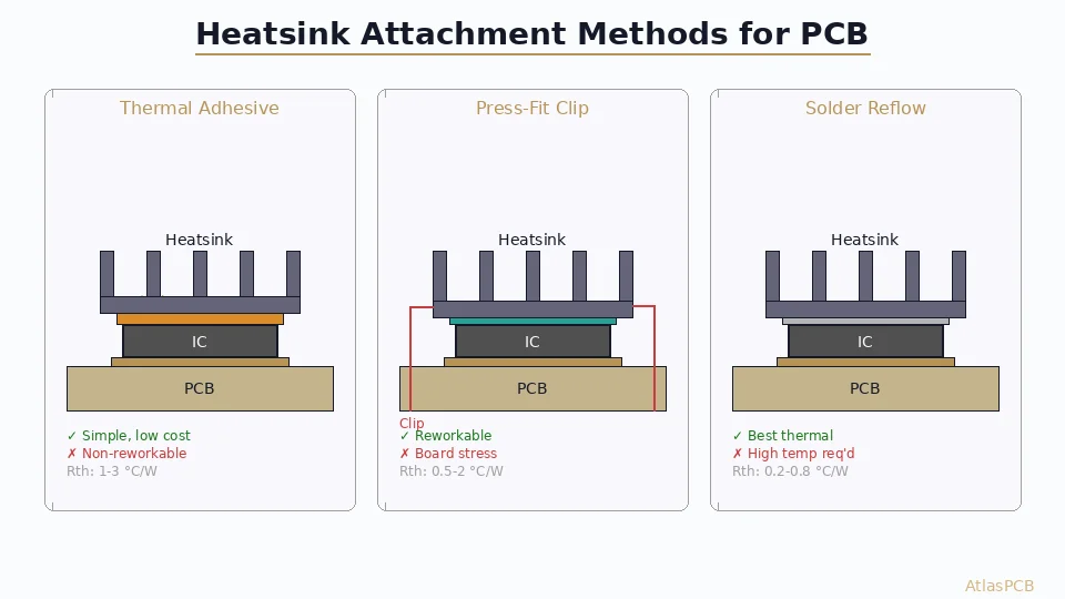
Thermal Resistance Comparison Summary
| Method | Rcs (°C/W) | Rework | Assembly Cost | Best For |
|---|---|---|---|---|
| Thermal tape | 2.0-4.0 | Difficult | Lowest | < 3W, prototypes |
| Thermal epoxy | 1.5-3.0 | No | Low | 3-10W, permanent |
| Clip + thermal pad | 0.5-2.0 | Easy | Medium | 10-50W, serviceable |
| Screw + grease | 0.2-0.8 | Easy | High | 20-100W+, high-rel |
| Solder reflow | 0.2-0.8 | Moderate | Medium | 5-50W, high-volume |
PCB Layout Considerations for Thermal Mounting
Copper Pour Under Heatsink
Regardless of attachment method, the PCB copper beneath the heatsink is critical:
- Full copper pour (no thermal relief) on the mounting layer
- Multiple thermal via arrays connecting to internal planes (0.3mm drill, 0.6mm center-to-center)
- Avoid routing traces under the heatsink pad area
- Ground plane connection provides both thermal and electrical benefit
Component Placement Near Heatsinks
- Maintain 3mm minimum clearance between heatsink body and adjacent components
- Account for heatsink dimensional tolerance (±0.5mm typical)
- Consider airflow path — don’t block inlet/outlet with tall components
- Temperature-sensitive components (crystals, electrolytic capacitors) should be positioned upstream in airflow
Reliability and Lifetime Considerations
Thermal Cycling Performance
Each method responds differently to repeated temperature cycles (e.g., -40°C to +85°C industrial range):
- Thermal adhesive: Degrades after 500-2000 cycles due to CTE mismatch stress. Epoxy can crack; tape can delaminate.
- Mechanical clips: Minimal degradation. Spring force remains constant. Thermal pad may thin over time but remains functional.
- Solder reflow: Subject to solder fatigue similar to BGA joints. Large solder area distributes stress effectively. Typically >5000 cycles with proper voiding control.
Vibration Resistance
- Adhesive: Good for light heatsinks (<10g). Heavy heatsinks can peel under vibration.
- Mechanical: Best vibration resistance with proper spring force.
- Solder: Good for moderate vibration. Not recommended for sustained high-g environments without underfill support.
Further Reading
- Thermal Via Array Design Rules for PCB Power Electronics — Optimizing via patterns under thermal pads
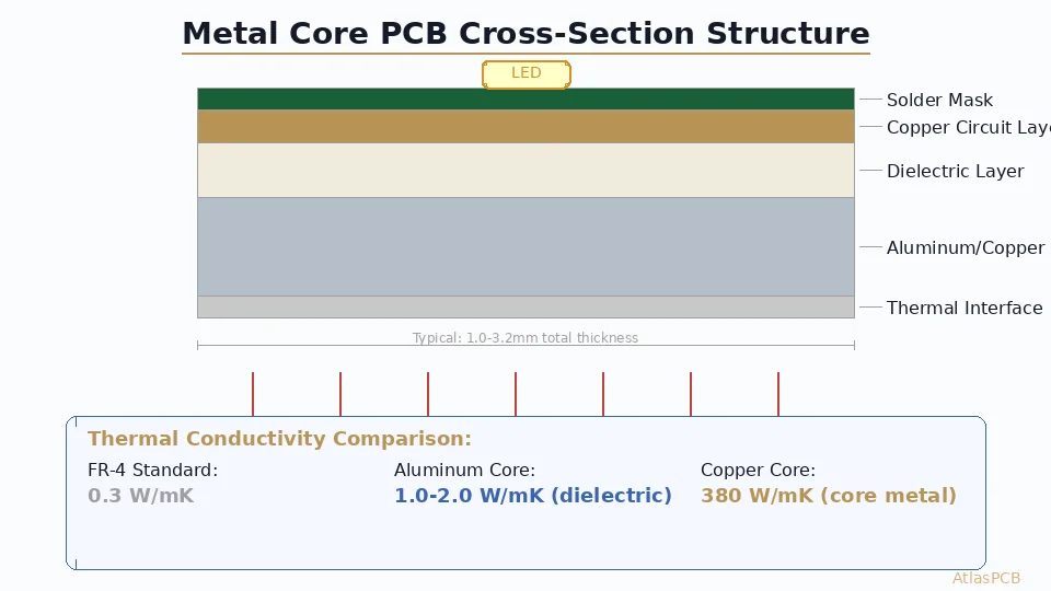
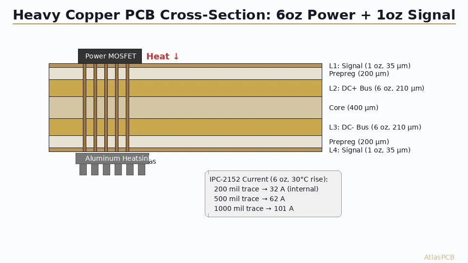
- Heavy Copper PCB Design for Power Electronics — When standard 1oz copper isn’t enough
- PCB CTE Mismatch and Thermal Stress in Multilayer Boards — Understanding material expansion failures
- VIPPO Via-in-Pad Plated Over Design Guide — Preventing solder wicking in thermal pads
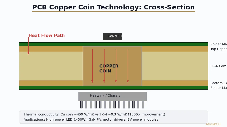
Designing a high-power PCB? AtlasPCB specializes in thermal management solutions including heavy copper (up to 6oz), embedded copper coins, and precision thermal pad design. Our DFM review catches thermal issues before they become field failures. Request thermal design support →
About AtlasPCB — We specialize in complex PCB manufacturing for HDI, RF, and high-reliability applications. Explore our RF and high-frequency PCB services, PCB assembly services, or get an aluminum and metal-core PCB services . Every order includes free engineering review. Get your quote.
Reviewed by AtlasPCB Engineering Team — IPC-certified manufacturing specialists with 15+ years of production experience in HDI, RF, and high-reliability PCB fabrication. Content based on factory floor data and real customer design reviews.
- thermal-management
- heatsink
- thermal-interface
- pcb-assembly
- power-electronics