· AtlasPCB Engineering · Engineering · 13 min read
Buried Via Technology in High-Density PCBs: Design Rules, Fabrication & Cost
Comprehensive guide to buried via technology in HDI PCBs. Learn design rules, fabrication sequences, cost drivers, and when buried vias outperform through-hole alternatives.
Introduction: When Through-Holes Are Not Enough
As electronic products shrink and functionality increases, PCB designers face an increasingly common dilemma: there is not enough routing space to connect all the nets using conventional through-hole vias. Through-hole vias consume real estate on every layer of the board, creating keep-out zones that block routing channels from top to bottom.
Buried via technology solves this problem by confining interconnections to the internal layers where they are needed, freeing up routing channels on other layers. Combined with [blind vias]/blog/blind-via-vs-buried-via/), buried vias are a foundational element of high-density interconnect (HDI) PCB construction.
This article provides a practical engineering guide to buried via technology — covering when to use them, how to design with them, what they cost, and how they are fabricated. Whether you are transitioning from a 6-layer through-hole design to an 8-layer HDI build, or optimizing a complex 16-layer stackup, understanding buried vias will expand your design options significantly.
What Is a Buried Via?
A buried via is a plated hole that connects two or more internal layers of a PCB without extending to either outer surface. After fabrication, the via is completely encapsulated within the board laminate — invisible and inaccessible from the outside.
Buried Via vs. Other Via Types
| Via Type | Connects | Visible From | Fabrication |
|---|---|---|---|
| Through-hole via | All layers (top to bottom) | Both surfaces | Standard single drill + plate |
| Blind via | One outer layer to internal layer(s) | One surface | Sequential lamination or laser drill |
| Buried via | Internal layer to internal layer(s) | Neither surface | Sequential lamination required |
| Microvia | Adjacent layers only (one layer span) | Depends on location | Laser drill |
IPC Nomenclature
IPC-2315 and IPC-4104 define buried via configurations using layer-pair notation. For example, in an 8-layer board:
- Buried via L2-L7: Connects Layer 2 to Layer 7 (spans 6 layers internally)
- Buried via L3-L6: Connects Layer 3 to Layer 6 (spans 4 layers internally)
- Buried via L3-L4: Connects only Layer 3 and Layer 4 (single core)
The layer-pair notation is essential for communicating your design intent to the fabricator and must be clearly documented in the fabrication drawing.
When to Use Buried Vias
Design Scenarios That Benefit from Buried Vias
BGA escape routing: High pin-count BGAs (400+ pins at ≤0.8 mm pitch) often cannot be fully routed using only surface and through-hole vias. Buried vias between inner signal layers provide additional escape channels without consuming surface routing space.
Layer count reduction: A design that requires 12 layers with through-hole vias might fit in 8 layers with buried vias, because internal routing channels are freed from through-hole blockages. The layer count reduction can offset the additional processing cost.
Impedance-critical routing: Through-hole vias passing through reference planes create anti-pads that disrupt ground plane continuity. Buried vias that only span the required layers cause fewer reference plane disruptions, improving [signal integrity]/blog/signal-integrity-pcb-design-guide/).
Mixed-technology stackups: Designs that combine high-speed digital, RF, and power sections often benefit from buried vias that provide interconnection within each technology zone without interfering with others.
Size-constrained designs: When the board area is physically limited (wearables, implantable medical devices, aerospace), buried vias recover the routing density that through-hole vias consume.
When Buried Vias Are Overkill
- Low pin-count designs (<200 pins total) that can be routed with through-hole vias
- Cost-sensitive consumer products where the 30-80% cost increase is not justified by size or performance requirements
- Prototyping and low-volume where fabrication lead time is critical (buried vias add 3-5 days)
- Simple 2-4 layer designs where routing density is adequate
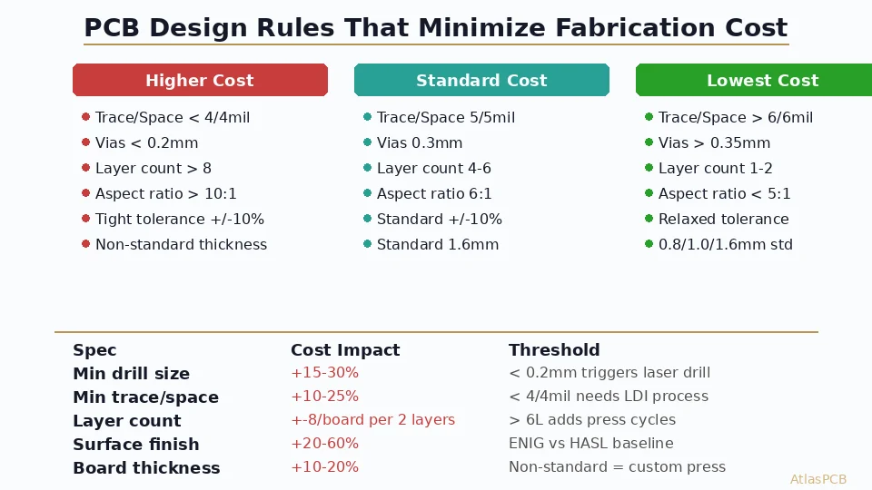
Buried Via Design Rules
Drill Diameter
| Process | Minimum Drill | Typical Drill Range | Notes |
|---|---|---|---|
| Mechanical drilling | 0.15 mm (6 mil) | 0.20-0.30 mm (8-12 mil) | Standard buried via process |
| Laser drilling | 0.075 mm (3 mil) | 0.075-0.15 mm (3-6 mil) | For single-span core vias only |
| Controlled-depth drill | 0.20 mm (8 mil) | 0.25-0.35 mm (10-14 mil) | Less common for buried vias |
Design rule: Use 0.20 mm (8 mil) minimum drill for standard buried vias. Reserve 0.15 mm (6 mil) for high-density applications where the fabricator has confirmed capability.
Aspect Ratio
The aspect ratio for buried vias is calculated using the sub-lamination thickness, not the total board thickness:
Aspect Ratio = Sub-lamination thickness / Drilled hole diameter
For example, a buried via L3-L6 in a board where the L3-L6 sub-lamination is 0.80 mm thick, drilled at 0.20 mm:
- Aspect ratio = 0.80 / 0.20 = 4.0:1 ✓ (comfortable)
Design rule: Keep buried via aspect ratio below 8:1. For optimal plating uniformity, target below 6:1. Consult the fabricator for aspect ratios above 8:1.
Annular Ring
| Parameter | IPC Class 2 | IPC Class 3 |
|---|---|---|
| External annular ring | ≥0.05 mm (2 mil) | ≥0.05 mm (2 mil) |
| Internal annular ring | ≥0.025 mm (1 mil) | ≥0.050 mm (2 mil) |
| Breakout allowed | Tangency or 90° breakout | No breakout |
Design rule: For buried vias, design the annular ring based on the sub-lamination registration tolerance (typically ±0.050 mm). A nominal annular ring of 0.125 mm (5 mil) provides adequate margin for most fabricators.
Pad and Anti-Pad Sizing
- Buried via pad diameter: Drill + 2 × annular ring + registration tolerance
- Example: 0.20 mm drill + 2 × 0.125 mm + 0.10 mm tolerance = 0.55 mm pad
- Anti-pad (clearance hole in planes): Pad diameter + 2 × minimum clearance
- Example: 0.55 mm pad + 2 × 0.20 mm = 0.95 mm anti-pad
- Anti-pads only exist on layers the buried via passes through — layers above and below the buried via range are unaffected
Stackup Registration
Buried vias are drilled in sub-laminations before the full board is assembled. Registration accuracy within a sub-lamination (typically ±0.050 mm / 2 mil) is better than full-stackup registration (typically ±0.075-0.100 mm / 3-4 mil) because:
- Fewer layers mean less cumulative registration error
- The sub-lamination is thinner and easier to handle
- Drilling occurs on a flat, uniform substrate
This tighter registration is one advantage of buried vias — it allows smaller pads and higher routing density on the internal layers.
Fabrication Process
Sequential Lamination Overview
Buried vias require sequential lamination — the process of building the PCB in stages rather than in a single press cycle. A typical sequence for an 8-layer board with buried vias on L3-L6:
Step 1: Core Preparation
- Start with the L3-L6 core laminate (double-sided copper-clad)
- Image and etch the L3 and L6 circuit patterns
- Drill buried via holes through the L3-L6 core
- Plate the buried vias (electroless + electrolytic copper)
- Image and etch the outer patterns of the sub-lamination (if needed for L3/L6 traces)
Step 2: Layup 6. Stack the completed L3-L6 sub-lamination with prepreg and outer cores 7. L1-L2 core on top, L7-L8 core on bottom, with prepreg between each layer set
Step 3: Final Lamination 8. Press the full stackup in a lamination press (180-200°C, 300-400 psi) 9. Drill through-hole vias and blind vias (if any) 10. Plate through-hole vias 11. Image and etch outer layers (L1, L8) 12. Complete standard PCB fabrication (solder mask, silkscreen, surface finish)
For a complete overview of the fabrication process, see our [PCB manufacturing process guide]/blog/pcb-manufacturing-process-15-steps/).
Multiple Buried Via Configurations
Complex designs may require multiple sets of buried vias at different layer pairs. Each set requires its own sub-lamination cycle:
Example: 12-layer board with buried vias L2-L5 and L8-L11:
| Step | Operation | Layers Involved |
|---|---|---|
| 1 | Image/etch L2-L5 core | L2, L5 |
| 2 | Drill + plate buried vias | L2-L5 |
| 3 | Image/etch L8-L11 core | L8, L11 |
| 4 | Drill + plate buried vias | L8-L11 |
| 5 | Layup + laminate all cores | L1-L12 |
| 6 | Drill + plate through-hole vias | L1-L12 |
| 7 | Final processing | L1, L12 |
Each additional buried via pair adds one drill/plate cycle and may add one lamination cycle, driving up cost and lead time.
Critical Process Controls
Registration: Each sub-lamination must maintain registration to ensure buried via pads align with the final-drill through-hole vias and blind vias that connect to them.
Resin fill: During final lamination, prepreg resin must completely fill the buried via holes. Incomplete fill creates voids that can trap moisture and cause reliability failures. Resin plugging or vacuum-assisted lamination is sometimes required.
Copper plating in buried vias: Must meet the same IPC-6012 thickness and ductility requirements as through-hole vias. The sub-lamination is typically thinner, so aspect ratios are favorable, but plating uniformity must still be verified by microsection.
Planarity: After sequential lamination, the board surface must be flat enough for subsequent processing. Buried via locations can create slight surface dimples if resin fill is insufficient.
Stackup Design with Buried Vias
Common Buried Via Stackup Configurations
8-layer with buried vias L3-L6:
L1: Signal (top)
L2: Ground
   --- buried via L3-L6 ---
L3: Signal
L4: Power
L5: Ground
L6: Signal
   --- end buried via ---
L7: Power
L8: Signal (bottom)
10-layer with buried vias L2-L9:
L1: Signal (top)
   --- buried via L2-L9 ---
L2: Ground
L3: Signal
L4: Power
L5: Ground
L6: Power
L7: Signal
L8: Ground
L9: Signal
   --- end buried via ---
L10: Signal (bottom)
12-layer with multiple buried via pairs:
L1: Signal (top)
L2: Ground
   --- buried via L3-L4 ---
L3: Signal
L4: Signal
   --- end buried via ---
L5: Power
L6: Ground
L7: Ground
L8: Power
   --- buried via L9-L10 ---
L9: Signal
L10: Signal
   --- end buried via ---
L11: Ground
L12: Signal (bottom)
Use our [PCB stackup calculator]/blog/pcb-stackup-calculator/) to model impedance for stackups with buried vias, as the sub-lamination dielectric may differ from the main lamination prepreg.
Impedance Considerations
Buried vias affect impedance in two ways:
Anti-pad voids: Where buried vias pass through reference planes, the anti-pad creates a local void in the ground or power plane. This void slightly increases the impedance of any trace routed near the anti-pad.
Via stub: Unlike through-hole vias, buried vias have no stubs — they connect only the layers they need to. This is a significant signal integrity advantage at frequencies above 3 GHz, where through-hole via stubs create resonances that degrade channel performance.
For high-speed design where via stubs are a concern, buried vias (combined with blind vias from the surface) can eliminate the need for back-drilling, saving cost and improving reliability.
Cost Analysis
Cost Drivers
| Factor | Cost Impact | Notes |
|---|---|---|
| Number of sequential laminations | High | Each cycle adds ~15-25% to base cost |
| Number of buried via drill sets | Moderate | Each drill set = additional drill program + plating |
| Buried via hole count | Low-Moderate | More holes = more drill time, but marginal per-hole cost is low |
| Aspect ratio complexity | Low | Only a factor at extreme ratios (>10:1) |
| Registration requirements | Moderate | Tighter specs require better equipment and more rejects |
Cost Comparison Examples
| Configuration | Approximate Cost Premium vs. Through-Hole Only |
|---|---|
| 8L with buried vias (1 pair: L3-L6) | +30-40% |
| 10L with buried vias (1 pair: L3-L8) | +25-35% |
| 8L with buried + blind vias | +50-70% |
| 12L with 2 buried via pairs | +60-80% |
| 16L with 3 buried via pairs | +80-120% |
Cost Optimization Strategies
Minimize buried via pairs: Each unique layer-pair configuration adds a sequential lamination cycle. Consolidate buried via connections to as few layer pairs as possible.
Consider layer count trade-off: Adding 2 layers (with through-hole vias only) might be cheaper than buried vias if the extra routing space is sufficient. Compare: 10-layer through-hole vs. 8-layer with buried vias.
Use buried vias selectively: Not every net needs a buried via. Reserve them for the routing bottleneck areas (BGA fanout, congested bus interfaces) and use through-hole vias elsewhere.
Combine with microvias: In HDI builds, laser-drilled microvias on outer layers combined with buried mechanical vias on inner layers can be more cost-effective than buried vias that span many layers.
Panelize efficiently: Buried via boards benefit from larger panel sizes that amortize the sequential lamination cost over more boards.
For [HDI PCB designs]/blog/hdi-pcb-design-guide/) where buried vias are part of a broader high-density strategy, the cost premium is often offset by the board size reduction or layer count savings.
Reliability Considerations
Thermal Cycling
Buried vias are subject to the same thermal cycling stresses as through-hole vias, but with some advantages:
- Lower aspect ratio: Sub-lamination thickness is less than total board thickness, resulting in lower aspect ratios and better plating uniformity
- Constrained z-axis expansion: The buried via is surrounded by laminate on all sides, which constrains z-axis movement compared to a through-hole via that spans the full board
- Resin fill support: If the buried via is fully filled with resin during lamination, the fill material supports the barrel against z-axis strain
Potential Failure Modes
Resin void at buried via: Incomplete resin fill during lamination creates a void that can absorb moisture and cause conductive anodic filament (CAF) growth or delamination under thermal stress.
Registration miss: If the through-hole or blind via that connects to the buried via is misregistered, the electrical connection may be marginal or open. This is tested with standard continuity/isolation testing.
Plating quality: The buried via plating is deposited before final lamination and cannot be inspected afterward without destructive microsection analysis. Process monitoring coupons are essential.
Delamination at buried via interface: The interface between the buried via sub-lamination and the prepreg added during final lamination is a potential delamination site if surface preparation is inadequate.
For comprehensive reliability testing approaches, see our [PCB testing methods guide]/blog/pcb-testing-methods/).
Design for Manufacturing (DFM) Guidelines
Fabrication Drawing Requirements
Your fabrication drawing must clearly specify:
- Layer assignments: Which layers each buried via connects (e.g., “Buried via L3-L6”)
- Drill table: Separate entries for buried via drills, through-hole drills, and blind via drills, with layer span noted
- Stackup diagram: Cross-section showing all via types and their layer spans
- Plating requirements: Copper thickness specifications for buried vias (per IPC-6012 class)
- Impedance tables: If buried vias affect controlled impedance structures
Common DFM Issues
- Buried via too close to through-hole via: The anti-pads can overlap, creating copper isolation issues. Maintain ≥0.25 mm clearance between buried via pad edge and through-hole via pad edge.
- Buried via under BGA pad: Ensure the buried via pad does not interfere with the BGA land pattern on the surface layer. A through-hole via or blind via typically connects the BGA pad to the buried via through an intermediate trace.
- Teardrop connections: Add teardrops at buried via pad-to-trace junctions to improve manufacturing yield.
For a comprehensive review of manufacturing constraints, consult our [DFM checklist]/blog/pcb-dfm-checklist/).
Emerging Trends in Buried Via Technology
Any-Layer HDI
Modern HDI processes enable vias between any pair of adjacent layers using laser drilling and sequential buildup. This “any-layer” approach effectively makes every via a form of buried or blind via, providing maximum routing flexibility. The tradeoff is cost: any-layer HDI with 3+ sequential buildup cycles can cost 3-5× a standard through-hole board.
Via-in-Pad with Buried Via Combination
Advanced designs combine [via-in-pad]/blog/via-in-pad-design/) technology on the surface with buried vias internally. The surface via-in-pad provides direct component connection, while the buried via provides internal layer routing without consuming surface area.
Copper-Filled Buried Vias
For power delivery or thermal management, buried vias can be filled with copper (via copper plating fill) to reduce resistance and improve thermal conductivity. This is particularly useful in power PCBs where buried vias carry significant current between internal power layers.
Conclusion
Buried via technology is a powerful tool for PCB designers facing routing density challenges. By confining interconnections to the internal layers where they are needed, buried vias free up routing channels on other layers and enable more compact, higher-performance designs.
The decision to use buried vias should be based on a clear cost-benefit analysis: the 30-80% fabrication cost premium must be justified by board size reduction, layer count savings, signal integrity improvement, or routing impossibility with through-hole-only construction. When the analysis favors buried vias, proper design rule adherence and clear fabrication documentation ensure that the manufacturing process delivers reliable results.
At Atlas PCB, our engineering team has extensive experience with buried via fabrication across all complexity levels. We can review your stackup, recommend the most cost-effective via strategy, and ensure your design meets both performance and manufacturability requirements.
Atlas PCB specializes in HDI PCB fabrication with buried via, blind via, and any-layer construction capabilities. Contact us for engineering support and a free DFM review on your next project.
Further Reading
- [PCB Copper Plating Process: Electroless vs Electrolytic Copper for HDI Vias and High-Density Interconnects]/blog/pcb-copper-plating-electroless-vs-electrolytic-hdi-vias/)
- [AI Hardware PCB Thermal Management: Advanced Multilayer Stackup Design for 1000W+ Processing Units]/blog/ai-hardware-pcb-thermal-management-multilayer-design/)
- [Rogers PCB Fabrication: Material Sourcing, Lead Times & Quality Control]/blog/rogers-pcb-fabrication/)
- [HDI PCB Design for 5G Antenna Integration: Signal Integrity Challenges in Millimeter-Wave Applications]/blog/hdi-5g-antenna-integration-pcb-design/)
- [PCB Via Size Guide: Mechanical, Laser & Microvia Dimensions]/blog/pcb-via-size-selection-guide/)
- Our Manufacturing Capabilities
About AtlasPCB — We specialize in complex PCB manufacturing for HDI, RF, and high-reliability applications. Explore our HDI PCB manufacturing capabilities, or get an multilayer PCB fabrication up to 30 layers . Every order includes free engineering review. Get your quote.
Reviewed by AtlasPCB Engineering Team — IPC-certified manufacturing specialists with 15+ years of production experience in HDI, RF, and high-reliability PCB fabrication. Content based on factory floor data and real customer design reviews.
- buried-via
- hdi
- high-density
- stackup