· AtlasPCB Engineering · Engineering · 8 min read
PCB Aspect Ratio in Drilling: Design Limits, Manufacturing Challenges, and Solutions for High-Layer-Count Boards
Understand PCB drill aspect ratio limits and their impact on plating quality. Learn IPC guidelines, mechanical vs laser drilling capabilities, and design strategies for reliable high-aspect-ratio vias in thick multilayer boards.
What Is Aspect Ratio in PCB Drilling?
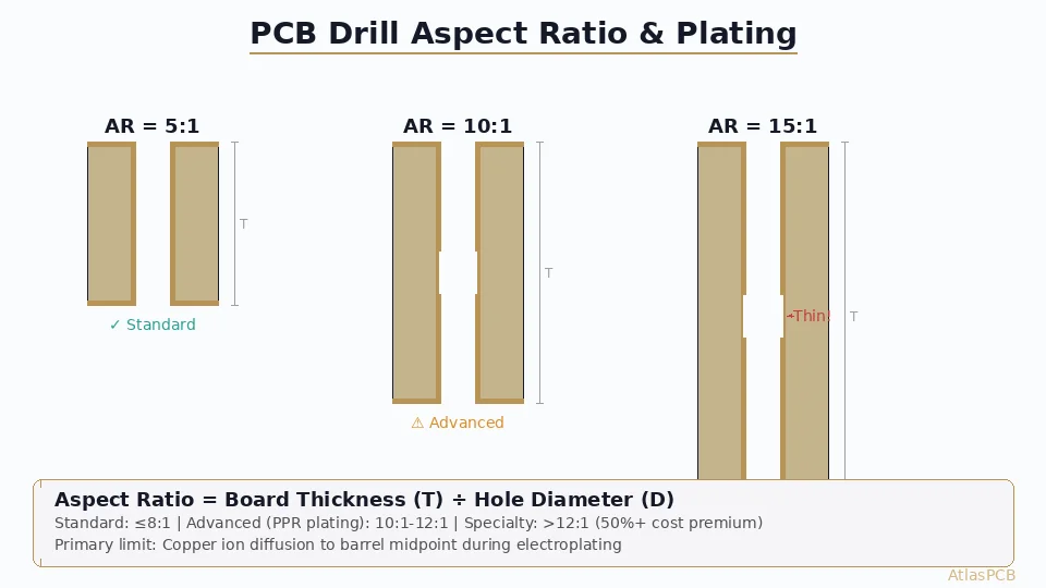
Aspect ratio in PCB manufacturing is defined as the ratio of the board’s total thickness to the finished hole diameter:
Aspect Ratio = Board Thickness ÷ Finished Hole Diameter
For example:
- 1.6 mm board, 0.3 mm hole → Aspect ratio = 5.3:1
- 2.4 mm board, 0.25 mm hole → Aspect ratio = 9.6:1
- 3.2 mm board, 0.2 mm hole → Aspect ratio = 16:1
The aspect ratio determines whether a plated through-hole (PTH) can be reliably manufactured with sufficient copper uniformity from top to bottom.
Why It Matters
The fundamental challenge is not drilling the hole — modern CNC machines can drill 0.15 mm holes in boards up to 6 mm thick. The challenge is plating the barrel with a uniform copper layer that meets IPC-6012 minimum thickness requirements (20–30 µm) at every point including the deepest midpoint of the barrel.
High aspect ratios create:
- Plating thickness gradient: Thick copper at hole entry, thin at midpoint
- Void risk: Gas bubbles trapped in deep barrels
- Reliability failure: Barrel cracks initiate at thinnest plating points during thermal cycling
IPC Standards and Aspect Ratio Limits
IPC-6012 Guidelines
IPC-6012 (Qualification and Performance Specification for Rigid Printed Boards) does not specify a hard maximum aspect ratio, but defines minimum plating thickness that becomes increasingly difficult to achieve at high ratios:
| Class | Minimum Barrel Copper | Typical Maximum AR |
|---|---|---|
| Class 1 (General) | 20 µm average | 8:1 |
| Class 2 (Dedicated) | 25 µm minimum | 10:1 |
| Class 3 (High-Reliability) | 25 µm minimum, no voids | 10:1 standard, 12:1 advanced |
IPC-2221B Design Guidelines
IPC-2221B Section 9.1.1 recommends:
- Maximum aspect ratio of 10:1 for standard production
- Design target of 8:1 or lower for best reliability
- Boards exceeding 10:1 should specify plating qualification coupons
IPC-6012 Class 3 Addendum
For defense/aerospace (IPC-6012DS):
- Barrel copper minimum: 25 µm with no single-point reading below 20 µm
- Void allowance: ≤ 5% of barrel length
- Ductility: ≥ 15% elongation at midpoint
- These requirements effectively limit practical AR to 10–12:1 without exotic plating
Mechanical Drilling Capabilities
Standard CNC Drilling
| Parameter | Standard | Advanced | Ultra-High |
|---|---|---|---|
| Minimum diameter | 0.15 mm | 0.10 mm | 0.075 mm |
| Maximum AR | 8:1 | 10:1 | 12:1+ |
| Drill speed | 80K–160K RPM | 100K–200K RPM | 200K–330K RPM |
| Hit count/drill | 500–3000 | 200–500 | 50–150 |
| Positional accuracy | ±50 µm | ±25 µm | ±15 µm |
| Board thickness range | 0.4–6.0 mm | 0.2–4.0 mm | 0.2–3.2 mm |
Drill Bit Selection for High AR
- Standard carbide: AR ≤ 8:1. Flute length limits chip evacuation in deeper holes.
- Extended flute: AR 8:1–12:1. Longer spiral flute allows chips to exit from deeper holes.
- Pecking drill cycle: AR 10:1–15:1. Drill retracts multiple times during each hole to clear chips.
- 2-peck cycle: Drill to 50%, retract, drill to 100%
- 3-peck cycle: Drill at 33%, 66%, 100% with full retraction
- Each peck adds ~0.5 seconds per hole — significant time impact on high-hole-count boards
Drill Wander and Wall Roughness
At high aspect ratios, the drill bit can wander off-axis as it penetrates deeper layers:
- AR ≤ 8:1: Typical wander < 25 µm
- AR 8:1–10:1: Wander 25–50 µm (acceptable for most designs)
- AR 10:1–12:1: Wander 50–75 µm (may affect annular ring compliance)
- AR > 12:1: Wander > 75 µm possible — risk of breakout on inner layers
Wall roughness also increases with AR due to multiple pecking cycles and chip re-cutting:
- Standard: Ra ≤ 20 µm
- High AR (>10:1): Ra 25–40 µm — rougher surface actually helps copper adhesion but may trap plating chemistry
Plating Challenges at High Aspect Ratios
The Midpoint Problem
The fundamental physics: electroplating depends on copper ion transport from bulk solution to the cathode surface (hole wall). In a deep, narrow hole, the only transport mechanism is diffusion — there is minimal convection inside the barrel.
Fick’s law limitation: The diffusion distance from hole entry to midpoint equals half the board thickness. At 10:1 AR with 3.2 mm board and 0.32 mm hole, ions must diffuse 1.6 mm through a 0.32 mm diameter channel. The plating rate at midpoint can be 40–60% lower than at the surface.
Throwing Power
“Throwing power” measures a plating bath’s ability to deposit uniform copper throughout high-AR holes. It’s expressed as a ratio:
Throwing Power = (Midpoint Thickness / Surface Thickness) × 100%
| Plating Method | Typical Throwing Power |
|---|---|
| DC acid copper (standard) | 60–70% |
| DC acid copper (optimized) | 70–80% |
| Periodic pulse plating | 80–90% |
| Pulse-reverse plating | 85–95% |
| Via-fill plating (PPR) | 90–100%+ |
For a 10:1 AR hole with target 25 µm minimum at midpoint:
- At 70% throwing power: Need to plate 36 µm at surface to get 25 µm at midpoint
- At 90% throwing power: Only need 28 µm at surface
Pulse-Reverse Plating
The most effective technique for high-AR holes uses periodic pulse reverse (PPR):
- Forward pulse (cathodic): 10–50 ms at 3–5 A/dm² → deposits copper
- Reverse pulse (anodic): 1–5 ms at 5–15 A/dm² → selectively dissolves surface copper (which is thicker)
- Net effect: Copper is redistributed from thick areas (hole entry) toward thin areas (midpoint)
PPR enables 12:1–15:1 AR with ≥90% throwing power, but adds:
- Equipment cost: PPR rectifiers 3–5× more expensive than DC
- Process time: 30–50% longer plating cycle
- Chemistry: Requires specific brightener/leveler additives tuned for PPR waveforms

Manufacturing High-Aspect-Ratio PCBs?
AtlasPCB's advanced plating lines support up to 12:1 aspect ratio with pulse-reverse plating and 100% cross-section verification. We manufacture 20+ layer boards for telecom, aerospace, and server infrastructure.
Get a Quote for Multilayer Boards →Laser Drilling and Aspect Ratio
CO₂ Laser
- Drills 75–300 µm diameter holes
- Maximum depth: ~200 µm (one layer of prepreg + copper)
- Effective AR: 2:1 to 3:1 (not an AR challenge — limited by depth, not ratio)
- Cannot drill through copper — requires conformal mask or copper window
UV Laser (Nd:YAG / Excimer)
- Drills 25–100 µm diameter holes
- Can ablate copper directly
- Maximum depth: ~150 µm
- Used for microvias in HDI sequential build-up
Laser Drilling AR Summary
Laser drilling inherently avoids high-AR problems because:
- Holes are shallow (typically one dielectric layer: 60–100 µm)
- Plating path is short — excellent throwing power even with DC plating
- Multiple stacked or staggered microvias replace one deep through-hole
Design Strategies to Avoid AR Issues
Strategy 1: HDI Sequential Build-Up
Replace through-holes with stacked microvias:
- Each via segment: 100–150 µm deep, 100 µm diameter → AR = 1:1 to 1.5:1
- Stack 3–4 microvias to span full board thickness
- Requires sequential lamination (adds fabrication cycles)
- Cost increase: 20–40% per additional lamination cycle
Strategy 2: Blind + Buried Via Architecture
Separate signal vias from power/ground:
- Signal vias: Blind (layers 1–4 only) → short barrel, low AR
- Power/ground: Through-hole but larger diameter (0.4+ mm) → acceptable AR
- Eliminates high-AR small-diameter through-holes entirely
Strategy 3: Back-Drilling (Controlled-Depth Drilling)
For high-speed designs where stub length matters:
- Drill full through-hole at standard AR-friendly diameter
- After plating, back-drill from one or both sides to remove unused barrel stub
- Effective electrical barrel length reduced without affecting plating quality
- Common in servers and telecom (PCIe Gen5/Gen6, 112G PAM4)
Strategy 4: Increase Hole Diameter
Sometimes the simplest solution:
- Increase via diameter from 0.2 mm to 0.3 mm → AR drops from 16:1 to 10.7:1
- Trade-off: Larger antipads, reduced routing density
- Often acceptable for power/ground vias where routing density pressure is lower
Strategy 5: Reduce Board Thickness
- Use thinner prepreg where possible
- Eliminate unnecessary copper layers
- Consider asymmetric stackup to reduce total thickness
- 2.8 mm → 2.4 mm with same 0.25 mm hole: AR drops from 11.2:1 to 9.6:1
Reliability Testing for High-AR Vias
Interconnect Stress Test (IST)
Per IPC-TM-650 Method 2.6.26:
- Rapid thermal cycling by resistive heating of test coupon
- Measures resistance change across daisy-chain through high-AR vias
- Pass: ≤ 10% resistance increase after 500 cycles (room temp to 150°C)
- High-AR vias typically fail IST before standard vias — midpoint thinning is the failure initiation site
Thermal Cycling
Per IPC-TM-650 Method 2.6.7:
- −55°C to +125°C, 30-minute dwells
- 500 cycles minimum for Class 3
- Cross-section after cycling to check for barrel cracks
- High-AR holes (>10:1): Specify 1000 cycles for qualification confidence
Cross-Section Analysis
The definitive test for high-AR plating:
- Section through hole center
- Measure plating thickness at: top entry, 25%, midpoint, 75%, bottom entry
- Midpoint must meet IPC-6012 minimum (25 µm for Class 2/3)
- Ratio of midpoint:surface should be ≥ 70% (good) or ≥ 85% (excellent)
Practical Examples
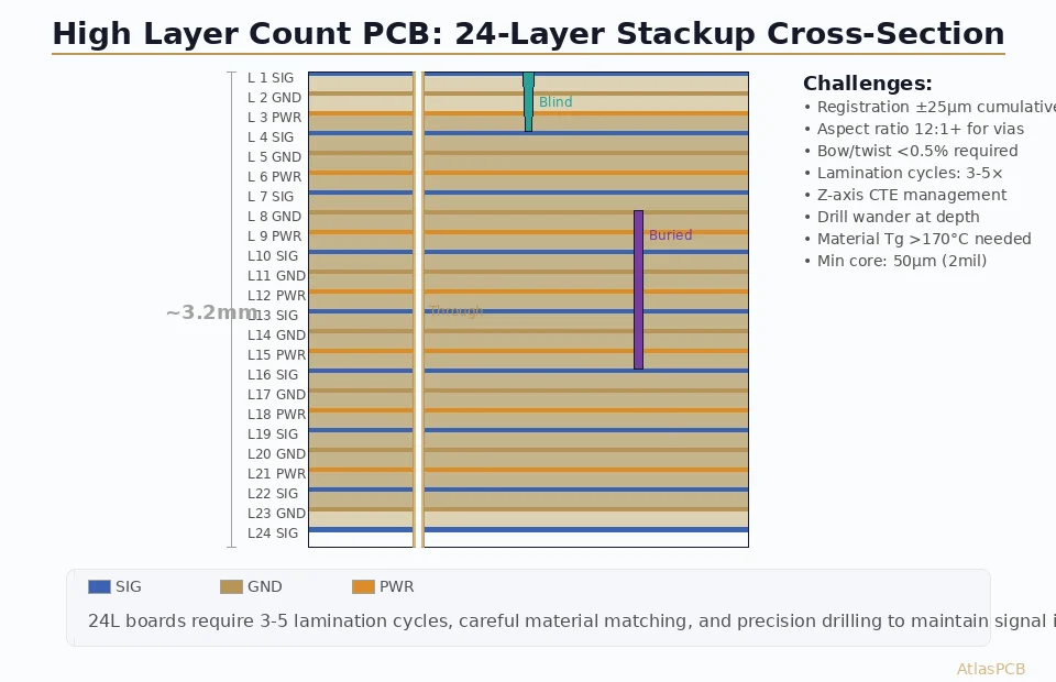
Example 1: 16-Layer Server Board
- Total thickness: 3.2 mm
- Through-hole requirement: 0.25 mm (for BGA escape)
- Calculated AR: 12.8:1 — exceeds standard capability
- Solution: HDI structure with blind vias (layers 1–4 and 13–16) + 0.35 mm through-holes for remaining connections → AR = 9.1:1
Example 2: 24-Layer Backplane
- Total thickness: 4.5 mm
- Signal vias: 0.25 mm → AR = 18:1 (impossible through-hole)
- Power vias: 0.45 mm → AR = 10:1 (achievable)
- Solution: Stub-free blind/buried structure for signals, through-hole for power + back-drill
Example 3: Aerospace Avionics Board
- Thickness: 2.4 mm, 12 layers
- Requirement: IPC-6012DS Class 3/A (25 µm min barrel, 20 µm single-point minimum)
- Hole diameter: 0.3 mm → AR = 8:1
- Approach: Standard plating with PPR, qualification coupon microsection, IST verification
Summary of Aspect Ratio Guidelines
| Board Thickness | Standard AR (8:1) | Advanced AR (10:1) | Specialty AR (12:1) |
|---|---|---|---|
| 1.0 mm | 0.125 mm min hole | 0.10 mm | 0.083 mm |
| 1.6 mm | 0.20 mm | 0.16 mm | 0.133 mm |
| 2.4 mm | 0.30 mm | 0.24 mm | 0.20 mm |
| 3.2 mm | 0.40 mm | 0.32 mm | 0.267 mm |
| 4.0 mm | 0.50 mm | 0.40 mm | 0.333 mm |
| 5.0 mm | 0.625 mm | 0.50 mm | 0.417 mm |
Design rule of thumb: Stay at 8:1 or below for lowest cost and highest reliability. Escalate to 10:1 only when density demands it. Beyond 10:1 requires explicit discussion with your fabricator and qualification testing.
Further Reading
- High-Layer-Count PCB Design and Manufacturing Challenges
- PCB Copper Plating: Electroless vs Electrolytic for HDI Vias
- PCB Back-Drilling for Via Stub Removal and Signal Integrity
- PCB Via Size Guide: Mechanical, Laser, and Microvia Dimensions
Designing high-layer-count PCBs with challenging aspect ratios? Talk to AtlasPCB Engineering — we provide fabrication DFM analysis, recommend optimal via architectures, and manufacture up to 68-layer boards with advanced plating processes.
About AtlasPCB — We specialize in complex PCB manufacturing for HDI, RF, and high-reliability applications. Explore our HDI PCB manufacturing capabilities, multilayer PCB fabrication up to 30 layers, or get an full PCB manufacturing capabilities . Every order includes free engineering review. Get your quote.
Reviewed by AtlasPCB Engineering Team — IPC-certified manufacturing specialists with 15+ years of production experience in HDI, RF, and high-reliability PCB fabrication. Content based on factory floor data and real customer design reviews.
- PCB drilling
- aspect ratio
- plating
- HDI
- multilayer PCB
- mechanical drilling
- laser drilling
- via design
- IPC-6012
- copper plating uniformity