· AtlasPCB Engineering · Engineering · 5 min read
Multilayer PCB Cost in 2026: Complete Pricing Analysis from 4-Layer to 20-Layer with Volume Scaling
Updated 2026 pricing analysis for multilayer PCBs covering 4 to 20+ layers. Includes real per-board cost ranges at prototype and production volumes, identifies the specific cost drivers at each layer count threshold, and provides actionable optimization strategies that reduce total fabrication spend by 15-35%.
2026 Pricing Table: Real Numbers from Production
Based on actual Q2 2026 production data from our facility. Standard FR-4 (Tg170), 1oz copper, standard through-hole vias, ENIG finish, 5/5mil trace/space.
Standard Board (100 x 100mm)
| Layers | 5 pieces | 10 pieces | 50 pieces | 100 pieces | 500 pieces | 1000 pieces |
|---|---|---|---|---|---|---|
| 4L | $18-30 | $12-25 | $8-15 | $5-10 | $3.50-6 | $2.50-4.50 |
| 6L | $30-50 | $22-42 | $14-25 | $9-16 | $6-10 | $4.50-7 |
| 8L | $50-80 | $35-60 | $22-38 | $14-24 | $9-15 | $7-11 |
| 10L | $70-110 | $50-85 | $32-52 | $20-35 | $13-22 | $10-16 |
| 12L | $100-160 | $70-120 | $45-72 | $28-48 | $18-30 | $14-22 |
| 16L | $160-260 | $120-200 | $75-120 | $48-78 | $30-50 | $22-36 |
| 20L | $250-400 | $180-350 | $110-180 | $72-115 | $45-72 | $35-55 |
Pricing reflects mid-2026 material costs including copper surcharge. Add 10-25% for impedance control, 25-50% for HDI vias, 15-30% for heavy copper (2oz+).
What Drives the Price Range Within Each Tier
The ranges above reflect variation in:
- Board size: Larger boards use more panel area (100x100mm is baseline; 200x150mm roughly doubles cost)
- Minimum features: 5/5mil = baseline; 4/4mil adds 10-20%; 3/3mil adds 25-40%
- Via density: More drilled holes = more drill time + more plating chemistry
- Copper weight: 1oz baseline; 2oz adds 15-25% (thicker copper requires longer etching)
- Special requirements: Controlled depth drilling, backdrilling, via fill → each adds 10-20%
The Four Cost Thresholds
Understanding where manufacturing process changes create step-function cost increases:
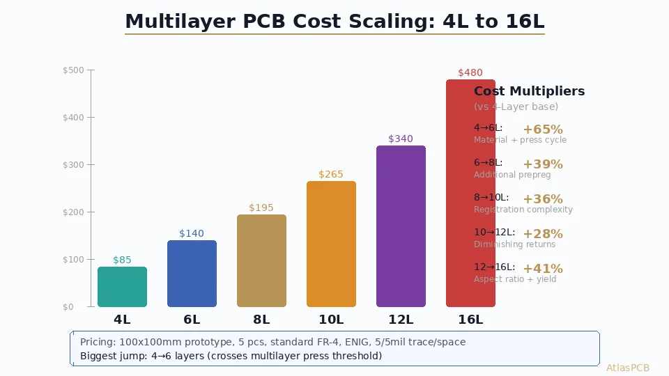
Threshold 1: 4 → 6 Layers (Biggest Percentage Jump)
Why: Transitions from single-press to multi-press lamination. A 4-layer board (outer-core-outer) is pressed in one cycle. Six layers require laminating inner cores, then pressing the complete stack — adding one full press cycle.
Cost impact: 40-65% increase over 4-layer.
Engineering question: Can you achieve the needed routing density on 4 layers by reducing trace/space? A 4-layer board at 4/4mil often provides equivalent routing density to a 6-layer at 6/6mil.
Threshold 2: 8 → 10 Layers (Registration Tolerance)
Why: Above 8 layers, maintaining layer-to-layer registration within +/-3mil across all layers becomes challenging. The cumulative registration error from multiple press cycles can exceed drilling tolerance, requiring tighter (more expensive) process control.
Cost impact: 30-45% increase over 8-layer.
Threshold 3: 12 → 14 Layers (Sequential Lamination)
Why: Many fabricators transition to sequential lamination (pressing in stages, not all at once) at 14+ layers. This adds 2-3 additional press cycles with alignment verification between each.
Cost impact: 25-35% increase over 12-layer.
Threshold 4: 20+ Layers (Specialized Equipment)
Why: Above 20 layers, board thickness exceeds 3.0mm for standard stackups, requiring high-aspect-ratio drilling (>12:1), specialized presses with extended dwell times, and very tight registration across multiple sequential lamination steps.
Cost impact: Variable but typically 50-100% increase over 16-layer.
💰 Get Exact Pricing for Your Layer Count
These are typical ranges — your specific board geometry, features, and volume determine actual price. Upload your Gerber files for an instant quote with full cost breakdown by layer, material, and finish. Get your multilayer PCB quote →
7 Strategies to Reduce Multilayer Cost
1. Increase Minimum Trace/Space (Saves 10-25%)
Moving from 4/4mil to 5/5mil reduces etching difficulty and improves yield. If your routing density allows it, this is free money — no performance impact on most designs below 5 GHz.
2. Standard Via Sizes (Saves 5-15%)
Using 10-mil or 12-mil finished holes (standard drill sizes) instead of 8-mil saves drilling time and improves plating yield. Smaller vias require more precise drilling and longer plating cycles.
3. Optimize Panel Utilization (Saves 10-20%)
Work with your fabricator on board dimensions that maximize panel utilization. Standard panel is 18x24 inches (457x610mm). A board that’s 105x105mm wastes significant panel area compared to 100x100mm — a 5mm dimension change can add one more board per panel and reduce per-unit cost by 10-15%.
4. Consolidate Layer Count (Evaluate 2 Fewer Layers)
Before committing to 10 layers, seriously evaluate whether 8 layers with 4/4mil trace/space can route your design. The routing density gain from tighter features often offsets 2 layers — and saves 30-45% on fabrication.
5. Standard Copper Weight (Saves 15-25% vs Heavy Copper)
Unless your design requires high-current traces (>3A), stick with 1oz copper on all layers. Heavy copper (2oz+) requires longer etch times, wider trace/space minimums, and generates more yield loss.
6. Volume Commitment Pricing (Saves 15-30%)
If you know your annual volume, negotiate pricing based on the total commitment rather than individual PO quantities. A commitment to 5000 boards/year often unlocks the 1000-piece pricing tier even on smaller individual orders.
7. Reduce Drill Count (Saves 5-10%)
Every via is a drilled hole. Mechanical drilling is a significant portion of fabrication time for dense multilayer boards. Where possible, reduce via count through routing optimization — longer traces with fewer layer transitions often cost less than short traces with many vias.
📊 Compare Your Quote Against These Benchmarks
If your current quote exceeds the ranges above by more than 30%, there may be optimization opportunities we can identify. Our engineering team reviews designs for cost reduction as part of every quote. Request cost-optimized multilayer quote →
Material Cost Impact (Beyond Standard FR-4)
| Material | Cost Multiplier vs Std FR-4 | When Needed |
|---|---|---|
| Standard FR-4 (Tg150) | 1.0x (baseline) | General purpose below 3 GHz |
| High-Tg FR-4 (Tg170) | 1.1-1.2x | Lead-free assembly, reliability |
| Mid-loss (Megtron 4, I-Speed) | 1.5-2.5x | 10-25 Gbps digital signals |
| Low-loss (Megtron 6, I-Tera) | 2.5-4.0x | 25-56 Gbps, very long traces |
| Ultra-low-loss (Megtron 7) | 4.0-6.0x | 112G PAM4, > 56 Gbps |
| Rogers RO4350B | 3.0-5.0x | RF/microwave below 20 GHz |
| PTFE (RT5880, TLY-5) | 8.0-15.0x | mmWave above 20 GHz |
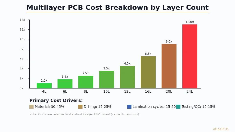
For most multilayer boards under 12 layers, material cost is 15-25% of total fabrication cost. At higher layer counts (16+), material becomes a larger fraction (25-40%) because the raw material stack is thicker and more expensive.
Summary
Multilayer PCB cost follows a predictable pattern driven by press cycles, registration tolerance, and yield management. Knowing where the step-function thresholds lie helps you design for the sweet spots: stay at or below process transition points when possible, and invest in layer count only when routing density genuinely demands it.
The best cost optimization starts at the design phase — not after you receive a quote that makes your finance team nervous.
Related Reading
About AtlasPCB — We specialize in complex PCB manufacturing for HDI, RF, and high-reliability applications. Explore our multilayer PCB fabrication up to 30 layers, or get an instant online PCB quote . Every order includes free engineering review. Get your quote.
Reviewed by AtlasPCB Engineering Team — IPC-certified manufacturing specialists with 15+ years of production experience in HDI, RF, and high-reliability PCB fabrication. Content based on factory floor data and real customer design reviews.
- multilayer PCB cost
- PCB pricing
- PCB fabrication cost
- layer count pricing
- PCB cost optimization
- volume pricing