· AtlasPCB Engineering · Engineering · 10 min read
PCB Design Rules for Minimum Fabrication Cost: A DFM Guide for Engineers Ordering Boards
Practical DFM guidelines that directly reduce PCB fabrication price. Covers trace/space thresholds, drill sizes, layer count decisions, material selection, and panelization strategies that keep your board in standard manufacturing processes and away from premium pricing tiers.

Quick Answer: The 8 Rules That Cut PCB Cost
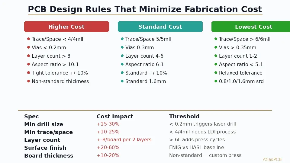
| Rule | Standard (Low Cost) | Premium (High Cost) | Cost Impact |
|---|---|---|---|
| Min trace/space | 5/5 mil or wider | < 4/4 mil | +10-25% |
| Min drill size | 0.3mm or larger | < 0.2mm (laser) | +20-40% |
| Layer count | 2 or 4 layers | 8+ layers | +$3-8/layer pair |
| Board thickness | 1.6mm standard | Non-standard | +10-20% |
| Surface finish | HASL or OSP | ENIG | +30-60% |
| Impedance control | None specified | +/-5% controlled | +10-25% |
| Aspect ratio | < 8:1 | > 10:1 | +15-30% |
| Panel utilization | > 80% material use | < 60% material use | +15-40% |
Follow these thresholds and your board stays in standard fabrication processes at every major PCB manufacturer. Cross any threshold and you enter premium pricing territory.
Understanding What Actually Drives PCB Price
Most engineers think of PCB cost as a black box — upload Gerbers, get a price. But fabrication cost is fundamentally determined by which manufacturing processes your design requires. Every PCB factory has a “standard” process window that handles the majority of orders with high yield and minimal setup. When your design falls outside that window, it triggers specialized equipment, slower processing speeds, or additional quality gates that directly increase cost.
The standard window at most Asian fabricators (where the majority of prototype and mid-volume boards are made) looks like this: 4/4mil trace/space, 0.2mm minimum drill, up to 8 layers, 1.6mm FR-4, HASL finish, no impedance control. Anything within this window gets processed in bulk on automated lines with minimal human intervention. Anything outside requires dedicated attention, specialty tooling, or premium materials.
The key insight for cost optimization is not to eliminate features you need — it is to avoid accidentally triggering premium processes when standard processes would work. Many engineers specify tighter tolerances than their circuit actually requires, simply out of habit or overly conservative design rules. Every unnecessary tight spec costs money.
COST-OPTIMIZED FABRICATION
Upload Your Design for Instant Pricing
Our quote engine identifies cost drivers in your Gerber files and suggests DFM optimizations that can reduce price by 20-40%.
Get Instant Quote ›Rule 1: Trace Width and Spacing — The LDI Threshold
The single most impactful cost variable in PCB imaging is whether your design can be processed with conventional phototool (film) exposure or requires laser direct imaging (LDI). Conventional film exposure handles 4/4mil (100/100um) trace/space reliably and costs essentially nothing extra per panel. Once you drop below 4/4mil, most fabricators switch to LDI — a sequential, slower process that adds 10-25% to the imaging cost per layer.
For designs that only need 5/5mil trace/space on signal layers, you are comfortably in the conventional process window. The sweet spot is 5/5mil for fine-pitch BGA escape routing and 6/6mil or wider everywhere else. If you only need tight trace/space in one small area (say, around a 0.5mm-pitch BGA), ask your fabricator if they can use conventional imaging with a local tolerance note — some will accommodate this without charging LDI rates for the entire board.
Ground and power planes do not require tight trace/space, so avoid applying your tightest design rule globally. Set your inner-layer ground planes to 8/8mil clearances and only apply 5/5mil rules on routing layers where you actually need the density.
Rule 2: Drill Size — Mechanical vs Laser Breakpoint
PCB drilling is priced in tiers based on the smallest hole in your design. Holes 0.3mm and larger are processed at full mechanical drill speed (typically 150,000-200,000 hits per spindle per hour). Between 0.2mm and 0.3mm, drill speed drops and bit breakage increases, adding roughly 10-15% to drilling cost. Below 0.2mm, you cross into the laser drilling domain — a fundamentally different process that adds 20-40% to via cost.
The practical implication: if your design has even one via at 0.15mm while the rest are 0.3mm, the entire panel may need laser processing for that layer pair. Design your via structure so that all vias on a given layer pair are above the mechanical threshold. If you truly need microvias for BGA escape, contain them to the HDI buildup layers and keep your core vias at 0.3mm or larger.
Another often-overlooked cost factor is drill aspect ratio. A 0.3mm hole through a 1.6mm board gives a 5.3:1 ratio — well within standard capability. But the same 0.3mm hole through a 3.0mm board gives 10:1 — pushing the limit of reliable mechanical drilling and triggering slower feed rates, reduced stack heights, and premium pricing. If your board is thick, size your vias proportionally.
Rule 3: Layer Count — Each Pair Is a Press Cycle
Every additional pair of signal layers adds a lamination cycle to the manufacturing process. A lamination cycle involves layup, vacuum press at elevated temperature (typically 180C for 90+ minutes), cool-down, and post-cure inspection. Each cycle adds roughly $3-8 per board at prototype quantities, and the yield risk compounds — an 8-layer board has three press cycles versus one for a 4-layer board, giving three opportunities for delamination, misregistration, or contamination.
The cost-optimization strategy is straightforward: use the minimum layer count that meets your routing requirements. A surprisingly large number of designs specified as 6-layer can be routed on 4 layers with slightly wider board dimensions or a few additional vias. Before committing to 6+ layers, try routing your critical nets on 4 layers. If you achieve 85%+ route completion, the remaining nets can often be accommodated by moving to slightly larger board outline or adding a small number of vias.
For HDI boards where you genuinely need 8+ layers with microvias, minimize the number of sequential lamination cycles. An “any-layer” HDI structure (where every layer has microvias) requires N-1 lamination cycles for N layers — dramatically more expensive than a standard through-hole multilayer with the same layer count. A 2+N+2 buildup (two HDI layers on each side of a conventional core) is typically 40-60% cheaper than a full any-layer structure with the same total layer count.
SMART LAYER COUNT SELECTION
Not Sure If You Need 4 or 6 Layers?
Upload your design. We provide stackup recommendations that balance signal integrity requirements against fabrication cost.
Compare Layer Options ›Rule 4: Material and Thickness Selection
Standard FR-4 at 1.6mm thickness is the default material for most PCB fabricators, and deviating from this baseline incurs surcharges at multiple stages. Non-standard thickness (0.4mm, 0.8mm, 2.0mm, 3.2mm) requires custom stackup design, potentially specialty prepreg combinations, and modified press recipes. The surcharge is typically 10-20% on material cost alone.
High-Tg FR-4 (Tg170 or above) adds 5-15% over standard Tg135-150 material. Unless your board will experience sustained temperatures above 130C in operation or you need enhanced CAF resistance for high-voltage applications, standard-Tg material is perfectly adequate. Many engineers reflexively specify High-Tg out of caution when their actual operating temperature never exceeds 85C.
Specialty laminates (Rogers, PTFE, polyimide, metal-core) carry substantial premiums — typically 3-10x the cost of FR-4 for the raw material. If your design only needs specialty material for one or two RF signal layers, consider a hybrid stackup where Rogers material is used only for the RF layers and standard FR-4 for the remainder. This can cut material cost by 40-60% compared to an all-Rogers construction.
Rule 5: Surface Finish and Special Processes
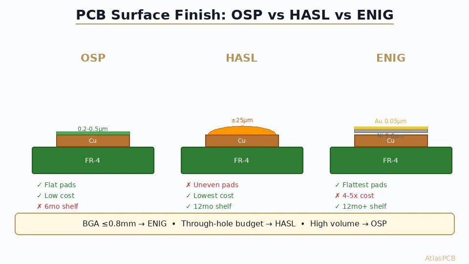
Surface finish is one of the easiest cost levers to pull because it has no impact on routing, stackup, or layer count. The cost hierarchy from cheapest to most expensive: HASL (baseline) < OSP (+5-8%) < Immersion Tin (+8-12%) < Immersion Silver (+15-25%) < ENIG (+30-60%) < Hard Gold (+80-200%, selective).
For prototypes and products that will be assembled within 30 days of fabrication, HASL or OSP are perfectly adequate and save significant cost. ENIG is only justified when you need the wire-bondability, the coplanarity for ultra-fine-pitch BGAs (< 0.4mm), or the shelf life for boards that may sit in inventory for 6+ months.
Other special processes that trigger premium pricing: controlled impedance testing (+10-25%), carbon ink printing (+15-25%), peelable solder mask (+10-15%), selective surface finish (+20-40%), and edge plating (+15-25%). Each of these is a separate processing step with setup cost. Only specify them when your design genuinely requires it.
Rule 6: Panelization for Maximum Material Utilization
Fabricators process boards in standardized panel sizes (typically 18x24 inches or 457x610mm). Your per-board price is heavily influenced by how efficiently your boards fit into the working panel. A small board (25x25mm) can fit 150+ per panel, giving excellent utilization. A board at 250x180mm might only fit 4 per panel with significant waste material.
The cost optimization is to design your board outline dimensions with panel utilization in mind. Sometimes adding 2-3mm to one dimension (which costs nothing functionally) allows one more row of boards per panel — reducing per-unit cost by 10-20%. Ask your fabricator for their panel size and work backwards to find the optimal board dimensions.
For small boards (under 50x50mm), panelization with V-score or tab routing is essential. Ordering individual small boards at prototype quantity is 3-5x more expensive per piece than ordering a panel with breakaway scoring. Most fabricators offer free panelization design — take advantage of it.
PANELIZATION OPTIMIZATION
We Optimize Your Panel Layout for Minimum Waste
Upload your board outline and we calculate the most efficient panelization with V-score or tab routing — maximizing boards per panel.
Get Panel Quote ›Putting It Together: A Cost-Optimization Checklist
Before submitting your design for quote, run through this checklist. Each item you can move from “premium” to “standard” typically saves 5-15% on the total board price:
- Can any trace/space be widened from 4/4mil to 5/5mil without functional impact?
- Are all vias 0.3mm or larger? Can any 0.2mm vias be eliminated or enlarged?
- Is the layer count the absolute minimum needed for routing and signal integrity?
- Can you use standard 1.6mm FR-4 thickness with Tg135-150?
- Does your assembly process really require ENIG, or will HASL/OSP work?
- Can you relax impedance tolerance from +/-5% to +/-10%?
- Is your board outline dimension optimized for fabricator panel utilization?
- Have you specified only the special processes (edge plating, carbon ink, backdrilling) that you actually need?
A design that answers “yes” to all eight questions will typically price 30-50% lower than one that specifies premium processes by default. The technical performance is often identical — you are simply avoiding paying for manufacturing precision your circuit does not require.
ATLASPCB
Get Your Optimized Price in 30 Seconds
Upload Gerbers. Our system auto-detects cost drivers and shows you exactly which specs are adding cost. Standard 5-18 day lead time, rush from 1 day.
Upload Gerber Files ›Related Reading:
About AtlasPCB — We specialize in complex PCB manufacturing for HDI, RF, and high-reliability applications. Explore our free engineering DFM review . Every order includes free engineering review. Get your quote.
Reviewed by AtlasPCB Engineering Team — IPC-certified manufacturing specialists with 15+ years of production experience in HDI, RF, and high-reliability PCB fabrication. Content based on factory floor data and real customer design reviews.
- pcb
- dfm
- cost-optimization
- design-rules
- manufacturing