· Engineering · 6 min read
Multilayer PCB Cost: 4-Layer vs 6-Layer vs 8-Layer Price Comparison and Optimization
Detailed cost comparison between 4-layer, 6-layer, and 8-layer PCBs. Understand the real cost drivers — layer count, material selection, via structure, and minimum trace — with actual pricing ranges and strategies to reduce per-board cost without sacrificing performance.
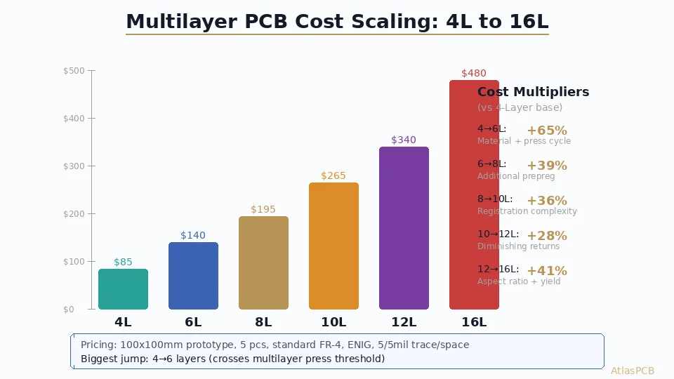
Quick Price Reference: 100x100mm Board, 10-Piece Prototype
| Layer Count | Price Range (per board) | Typical Lead Time | Key Cost Driver |
|---|---|---|---|
| 4-layer | $12-25 | 5-7 days | Standard — baseline |
| 6-layer | $22-42 | 7-10 days | Additional press cycle |
| 8-layer | $35-60 | 8-12 days | Material stack complexity |
| 10-layer | $50-85 | 10-14 days | Alignment tolerance |
| 12-layer | $70-120 | 12-16 days | Sequential lamination may be needed |
Note: Prices assume standard FR-4 (Tg150-170), 1oz copper, 5/5mil trace/space, ENIG finish, and standard mechanical drill. Prices for 2026 market conditions with standard copper foil pricing.
The Real Cost Drivers (Not Just Layer Count)
Layer count is the most visible spec, but these factors often have equal or greater cost impact:
1. Minimum Trace and Space
| Trace/Space | Yield Impact | Cost Multiplier |
|---|---|---|
| 5/5 mil (125um) | Standard yield | 1.0x (baseline) |
| 4/4 mil (100um) | Reduced yield, tighter process | 1.1-1.2x |
| 3.5/3.5 mil (90um) | Requires premium imaging | 1.2-1.4x |
| 3/3 mil (75um) | mSAP or laser direct imaging | 1.4-1.8x |
Practical takeaway: If you can route your 6-layer board at 4/4mil instead of 3/3mil, you may save 20-40% — equivalent to dropping back to a 4-layer price point.
2. Via Structure
| Via Type | Process | Cost Adder (vs standard PTH) |
|---|---|---|
| Standard through-hole (0.2-0.35mm) | Single drill | Baseline |
| Blind via (laser, 0.1mm) | Sequential lamination | +25-40% |
| Buried via | Additional press cycle | +20-30% |
| Stacked microvia (2+ levels) | Multiple sequential cycles | +50-100% |
| Via-in-pad (filled & capped) | Fill + planarize + cap plate | +15-35% |
| Backdrilling | Secondary operation | +10-20% |
3. Material Selection
| Material | Typical Application | Cost vs Standard FR-4 |
|---|---|---|
| Standard FR-4 (Tg150) | General purpose | 1.0x |
| High-Tg FR-4 (Tg170) | Lead-free assembly, automotive | 1.05-1.1x |
| Mid-loss (Megtron 4, IS415) | 10-25 Gbps signals | 1.5-2.0x |
| Low-loss (Megtron 6, IS680) | 25-56 Gbps signals | 2.5-3.5x |
| Rogers 4350B | RF/microwave layers | 3-5x (hybrid stackup common) |
| Polyimide (flex/rigid-flex) | Flex sections | 2-4x |
INSTANT MULTILAYER PRICING
See Your Exact Cost in 60 Seconds
Upload Gerber files or enter board specs to get instant pricing across 4, 6, 8, and 10-layer options. Compare stackups and material choices side by side.
Get Instant Quote ›Why the 4-to-6 Layer Jump Is Disproportionately Expensive
The cost curve from 4 to 6 layers is non-linear because of process changes:
4-layer fabrication:
- Single lamination press cycle
- Two inner layers imaged and etched on one core
- Core + prepreg + outer foil — straightforward stack
- Well-established, high-yield commodity process
- Most fabricators can produce on standard equipment
6-layer fabrication:
- Two lamination press cycles (or one with multiple cores)
- Four inner layers requiring alignment across three separate panels
- Tighter registration tolerance between layers
- More complex drill-to-copper clearance management
- Potentially requires different equipment class
This process threshold is why 6-layer boards aren’t simply “50% more copper = 50% more cost.” You’re paying for the process complexity jump, not just material.
From 6 to 8 layers, the incremental cost is more linear — you’re already in the multilayer process flow, and adding two more inner layers is an incremental material and registration effort.
Cost Optimization Strategies by Layer Count
Optimizing 4-Layer Cost
- Maximize panel utilization: Design board outline to tessellate efficiently on 18x24” (457x610mm) production panels
- Standard drill sizes: Use 0.2mm, 0.25mm, 0.3mm vias — non-standard sizes require tool changes
- Avoid mixed copper weights: 1oz all layers is cheapest; 2oz outer / 1oz inner adds 10-15%
- Standard thickness: 1.6mm is commodity; 0.8mm or 2.0mm costs more due to material availability
Optimizing 6-Layer Cost
- Choose between buried vias and standard through-hole: A 6-layer with only through-hole vias costs 30-40% less than one requiring buried vias between inner layers
- Consistent trace/space: If only one layer needs 3/3mil, the entire board is priced at 3/3mil imaging. Can you route that layer at 4/4mil?
- Standard stackup: 1.6mm with symmetric prepreg/core structure uses readily available materials
Optimizing 8-Layer Cost
- Avoid sequential lamination if possible: Route signals to eliminate buried/blind vias
- Use standard core thicknesses: 0.1mm, 0.2mm, 0.36mm, 0.5mm cores are commodity
- Consider whether you really need 8 layers: Sometimes a 6-layer with slightly larger board area is cheaper than squeezing into 8 layers with the same footprint
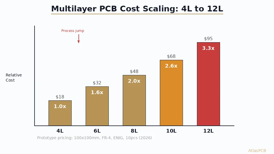
Volume Pricing: How Quantity Affects the Layer Count Decision
| Quantity | 4L Cost/Board | 6L Cost/Board | 8L Cost/Board |
|---|---|---|---|
| 5 pcs (prototype) | $18-25 | $30-42 | $45-65 |
| 50 pcs (pilot) | $8-12 | $14-20 | $22-32 |
| 500 pcs (production) | $3-5 | $5-8 | $8-13 |
| 5000 pcs (mass production) | $1.50-2.50 | $2.50-4.00 | $4.00-6.50 |
Note: Standard FR-4, 100x100mm board, ENIG finish. 2026 pricing.
Key insight: At high volumes, the per-board cost difference between 4-layer and 6-layer shrinks to $1-2. If adding 2 layers lets you reduce board area by 20%+, the smaller board with more layers can actually be cheaper per unit because you fit more boards per panel.
PRODUCTION VOLUME PRICING
Prototype to Mass Production, Competitive Pricing
From 1-piece prototypes to 10,000+ production runs. Multilayer boards up to 30 layers with 5-day express options for 4-layer and 7-day for 6-layer.
Compare Volume Pricing ›When to Step Up: Decision Framework
Stay at 4 Layers When:
- Component density allows comfortable routing at 5/5mil
- No controlled impedance requirements beyond 2 signal + 2 plane layers
- Board area is not constrained
- Power delivery doesn’t require dedicated plane pairs
- Budget is the primary constraint and performance is adequate
Move to 6 Layers When:
- BGA components require escape routing that 4 layers can’t accommodate
- Signal integrity requires dedicated ground reference planes for both signal layers
- Mixed-signal design needs analog/digital power plane separation
- Controlled impedance on all signal traces (stripline between planes)
- EMC requirements demand solid reference planes
Move to 8 Layers When:
- High pin-count processors (>400 pins) with multiple power domains
- DDR4/DDR5 routing requiring matched-length signal pairs with dedicated return planes
- Multiple high-speed interfaces (PCIe, USB3, Ethernet) on the same board
- RF + digital sections requiring isolation layers
- Dense BGA pitch (< 0.65mm) with standard through-hole construction
For guidance on designing your multilayer stackup, see our controlled impedance stackup design rules guide.
STACKUP CONSULTATION
Not Sure How Many Layers You Need?
Send your schematic or netlist — our engineers recommend the optimal layer count and stackup configuration that balances cost, performance, and manufacturing yield.
Get Stackup Advice ›Hidden Costs to Watch For
These specs silently inflate your multilayer quote:
- Copper weight mismatch — 2oz on outer + 1oz on inner requires process adjustment
- Aspect ratio — 8-layer at 1.6mm with 0.15mm vias = 10.7:1 aspect ratio (premium process)
- Impedance tolerance — +/-5% costs more than +/-10% (tighter press control)
- Non-standard thickness — 1.2mm or 2.4mm boards use custom core stacks
- Panel edge requirements — impedance coupons, TDR test points add panel area waste
ATLASPCB
Upload Your Design — Get Multilayer Pricing in Minutes
4 to 30 layers, standard FR-4 to Rogers hybrid stackups. Transparent pricing with no hidden fees. Lead times from 5 days.
Get Instant Quote ›Related Reading:
About AtlasPCB — We specialize in complex PCB manufacturing for HDI, RF, and high-reliability applications. Explore our multilayer PCB fabrication up to 30 layers, or get an instant online PCB quote . Every order includes free engineering review. Get your quote.
Reviewed by AtlasPCB Engineering Team — IPC-certified manufacturing specialists with 15+ years of production experience in HDI, RF, and high-reliability PCB fabrication. Content based on factory floor data and real customer design reviews.
- pcb-cost
- multilayer-pcb
- pcb-pricing
- stackup-design
- pcb-manufacturing