· AtlasPCB Engineering · Engineering · 11 min read
PCB Lead Times Explained: What Drives Turnaround and How to Get Boards Faster
A fabricator's perspective on what actually determines PCB manufacturing lead time. Understand the production steps, common delays, and practical strategies to shorten delivery without compromising quality.
Every hardware engineer has experienced the frustration of waiting for prototype boards. You finalize the layout on a Friday, send out Gerbers, and then spend the next week refreshing a tracking page. Understanding what happens inside the fabrication facility during that wait can help you make smarter decisions about your design and ordering process, potentially shaving days off your schedule without paying rush premiums.
This article looks at PCB lead time from the manufacturer’s side of the table. We will walk through the actual production sequence, identify where time gets consumed, and share practical strategies for getting boards into your hands faster.
The Production Clock Starts Later Than You Think
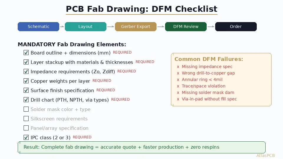
A common misconception is that manufacturing begins the moment you place an order. In reality, the clock does not start until your fabrication data passes engineering review. This front-end process involves a CAM engineer importing your Gerbers and drill files, verifying layer alignment, checking design rules against the factory’s process capabilities, and confirming that all specifications are unambiguous.
For straightforward designs with clean data, engineering review takes two to four hours. For complex boards with controlled impedance requirements, unusual stackups, or incomplete documentation, it can take one to two days. If the review reveals questions that require your input, the clock effectively pauses until you respond. This is why the single most effective way to shorten lead time has nothing to do with paying for expedited service. It is simply providing complete, unambiguous fabrication data from the start.
A well-prepared data package includes Gerber files for every copper and mask layer, an NC drill file with a tool table, a clear fabrication drawing specifying stackup, impedance targets, material, surface finish, and any special requirements, and an IPC netlist for electrical testing. When all of this arrives together and matches consistently, the board enters production within hours of order confirmation.
Where the Days Go: Understanding the Process Sequence
PCB fabrication is not a single manufacturing step but a chain of sequential processes, each requiring its own setup, processing time, and quality verification. For a standard 6-layer board with ENIG finish and controlled impedance, the production sequence looks roughly like this.
Inner layer imaging and etching is typically the first step after panel preparation, consuming about half a day. The imaged layers then go through automated optical inspection before lamination. Multilayer lamination itself is time-intensive because the press cycle runs for several hours under heat and pressure, and panels must cool gradually to avoid residual stress. For a 6-layer board, this means one lamination cycle. For an 8-layer board with buried vias, you may need two sequential lamination cycles, effectively doubling this phase.
After lamination, drilling is relatively fast for through-hole vias but becomes a bottleneck for HDI designs requiring laser drilling of microvias. A mechanical drill can process a panel in minutes, but laser drilling each microvia individually on dense HDI boards can take considerably longer, especially when multiple via layers require sequential drill-plate-laminate cycles.
Plating, outer layer imaging, etching, solder mask application, surface finish, electrical testing, and final inspection each add incremental time. The total accumulates to the published lead times that feel longer than any single step would suggest.
The Factors That Actually Move the Needle
Not all design choices affect lead time equally. Some specifications add a day; others add a week. Understanding the relative impact helps you make informed trade-offs during the design phase.
Layer count and sequential lamination represent the largest time variable. A 2-layer board skips the entire lamination process and can realistically be manufactured in a single day. Every additional pair of layers adds roughly one to two days because of the lamination cycle and the associated drilling and plating steps that follow. Boards requiring sequential lamination, such as those with buried vias or HDI structures with stacked microvias, multiply this effect because each lamination cycle must complete before the next buildup layer can begin.
Material availability is the silent schedule killer. Standard FR4 laminates like Shengyi S1000-2 and IT180A are stocked in large quantities at most Chinese fabricators. If your design specifies one of these materials, there is zero procurement delay. However, if you call out Rogers RO4350B, Panasonic Megtron 6, or Isola I-Tera MT40, the fabricator may need to order material from a distributor. For commonly used high-frequency materials like RO4350B and RO4003C, Atlas PCB maintains working stock precisely to eliminate this delay. For less common materials, procurement can add three to five working days before fabrication even begins.
Surface finish process time varies significantly between options. HASL (hot air solder leveling) and OSP (organic solderability preservative) are fast, single-step processes that add minimal time. ENIG (electroless nickel immersion gold) requires a multi-bath chemical deposition sequence and adds roughly a day to the schedule. Hard gold plating for edge connectors adds more because it requires selective masking and extended plating time to build up the required thickness. If your delivery timeline is extremely tight, specifying HASL or OSP where electrically acceptable is a straightforward way to recover half a day.
Via technology has a compounding effect on schedule. Through-hole vias are drilled in a single pass after final lamination and represent the fastest path. Blind vias require controlled-depth drilling or sequential lamination. Buried vias demand fabricating and plating an inner-layer sub-composite before the full lamination, adding an entire process loop. HDI microvias with stacked or staggered configurations involve multiple sequential drill-plate-fill-laminate cycles, each adding one to two days.
Common Causes of Unexpected Delays
Beyond design complexity, several practical issues frequently push deliveries beyond the quoted lead time. Being aware of these helps you prevent them.
Incomplete fabrication data is the number one cause. Missing drill files, ambiguous layer naming conventions, contradictory stackup information between the fab drawing and the Gerber set, or unspecified impedance coupling requirements all trigger engineering queries. Each query-response cycle can add a full working day if the designer is in a different time zone.
Design rule violations caught during DFM review are the second most common issue. Annular rings that fall below the factory’s minimum after drill registration tolerance, trace-to-edge clearances that are too tight for routing, or solder mask dams that are too narrow for reliable LPI application all require either a design revision or an explicit deviation acceptance. Factories will not proceed until this is resolved because manufacturing a board known to violate process limits risks a failed lot.
Material substitution discussions also consume time. If your design specifies a material that is out of stock and you have not pre-approved alternates, the factory must wait for your confirmation before proceeding with a different laminate grade. Specifying acceptable alternates on your fabrication drawing, such as noting that Shengyi S1000-2 or equivalent mid-Tg FR4 is acceptable, gives the factory flexibility to proceed without delay.
Practical Strategies for Faster Boards
Drawing from the production realities described above, here are the most effective approaches to minimizing lead time.
Design for standard process capabilities from the start. Using minimum trace and space of 4mil or wider, annular rings of 5mil or more, and standard drill sizes avoids the need for premium process lines and lets your board run on the factory’s highest-throughput equipment. Boards designed to standard rules can often be ganged onto shared production panels, which means they start processing faster because the factory does not need to wait for enough orders to fill a custom panel.
Provide fabrication-ready data with no ambiguity. A complete Gerber set using the RS-274X format with embedded apertures, a clearly labeled drill file in Excellon format, and a detailed fabrication drawing that specifies every parameter eliminates the engineering query cycle. If you use Altium, KiCad, or Eagle, their default Gerber output settings generally produce clean data. The common pitfalls are forgetting to include the board outline layer, omitting the drill file entirely, or leaving impedance values unspecified while noting that controlled impedance is required.
Choose stocked materials when possible. For most applications, standard FR4 delivers adequate performance through several gigahertz of bandwidth when paired with appropriate stackup design. If your design genuinely requires a specialty laminate, confirm availability with your fabricator before finalizing the design. A quick email asking whether RO4350B is in stock can save you a week of waiting.
Consolidate your specifications to standard options where the application allows. ENIG is an excellent surface finish, but if your board has no fine-pitch BGA pads and does not require the shelf life or planarity that ENIG provides, HASL-lead-free works perfectly and processes faster. Similarly, if your design can function with through-hole vias rather than blind or buried vias, the simpler via structure can reduce lead time by several days on complex multilayer boards.
Respond quickly to engineering queries. If a fabricator contacts you with a question about your design, responding within hours rather than days directly translates to faster delivery. Consider providing your mobile number or a messaging contact for time-sensitive projects, and let your fabricator know your time zone so queries can be timed to reach you during working hours.

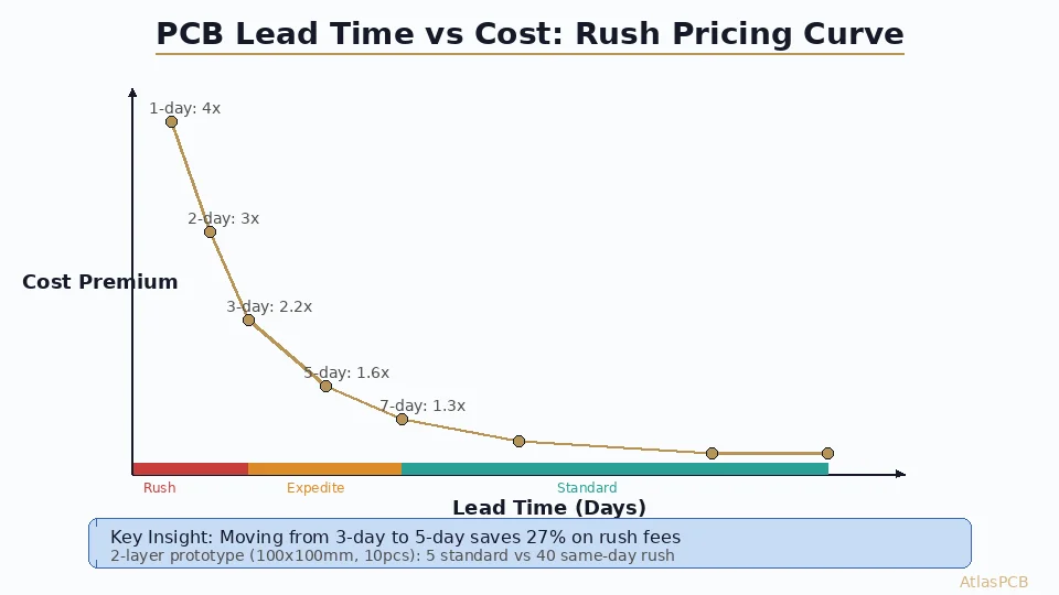
What Quick-Turn Really Means
Many fabricators advertise 24-hour or same-day PCB service, but it is worth understanding what that timeline actually covers. Quick-turn services typically apply to boards that meet a constrained set of specifications: two layers, standard FR4 at 1.6mm thickness, one-ounce copper, HASL finish, and minimum feature sizes well within standard process capabilities. Once you step outside these boundaries, adding layers, specifying controlled impedance, requiring blind vias, or selecting ENIG finish, the minimum achievable turnaround increases regardless of how much premium you pay.
The reason is physics and chemistry. Lamination press cycles cannot be rushed without compromising bond strength. Plating requires specific dwell times in chemical baths to achieve proper thickness and adhesion. Solder mask needs UV exposure and thermal cure cycles that cannot be shortened without risking adhesion failure. A reputable fabricator will not compromise these process parameters for speed because doing so creates reliability risks that surface weeks or months later in the field.
When a fabricator quotes a 5-day lead time for your 8-layer controlled-impedance board, that number represents the genuine minimum time required to manufacture it correctly. Paying for expedited service on such a board means your job gets priority scheduling at each process step rather than waiting in queue, but the actual processing time for each step remains the same.
Planning Ahead: The Best Schedule Strategy
The most effective approach to managing PCB lead time is not finding a faster fabricator but rather integrating realistic fabrication timelines into your project schedule from the beginning. If your design schedule assumes boards will arrive three days after Gerber release but your board actually requires ten days of fabrication plus three days of shipping, you have built a week of frustration into your plan.
For development projects with multiple revision cycles, consider releasing your first prototype as a simplified version. If your final design calls for eight layers with blind vias and ENIG, but you can validate the critical circuitry on a four-layer through-hole design with HASL, that first spin can arrive in half the time. Use the faster prototype to verify functionality, then commit to the full-complexity fabrication for the production-intent revision.
Maintaining a relationship with a fabricator who understands your typical designs also pays dividends over time. When your factory knows your design style, preferred materials, and standard specifications, their engineering review goes faster because the CAM team recognizes your data format and conventions. At Atlas PCB, repeat customers frequently see their boards enter production within hours of order placement because our engineering team already understands their requirements.
Summary
PCB lead time is not an arbitrary number set by the factory. It reflects the genuine time required to execute a sequence of chemical, mechanical, and inspection processes that produce a reliable circuit board. The primary drivers are layer count and lamination cycles, material procurement, via complexity, and the completeness of your design data.
The most impactful strategies for faster delivery are providing complete and unambiguous fabrication data, designing within standard process capabilities, choosing stocked materials, and building realistic timelines into your project schedule. When you need to push the boundaries, quick-turn service can prioritize your job through the production queue, but it cannot accelerate the underlying chemistry and physics of board fabrication.
Further Reading
About AtlasPCB — We specialize in complex PCB manufacturing for HDI, RF, and high-reliability applications. Explore our free engineering DFM review . Every order includes free engineering review. Get your quote.
Reviewed by AtlasPCB Engineering Team — IPC-certified manufacturing specialists with 15+ years of production experience in HDI, RF, and high-reliability PCB fabrication. Content based on factory floor data and real customer design reviews.
- pcb-manufacturing
- lead-time
- production
- DFM
- ordering-guide