· AtlasPCB Engineering · Engineering · 7 min read
Glass Core Substrates for Advanced PCB Packaging: Technology, Benefits, and Manufacturing Challenges
Explore how glass core substrates are transforming advanced packaging with ultra-low warpage, fine-pitch TGV interconnects, and superior dimensional stability for AI/HPC and RF applications.
The Rise of Glass Core Substrates in Advanced Electronics
The PCB and semiconductor packaging industries are experiencing a materials revolution. As AI accelerators demand ever-larger die sizes, finer interconnect pitches, and higher power densities, traditional organic substrates are reaching fundamental physical limits. Glass core substrates — using precision-formed borosilicate or alkali-free glass panels as the structural foundation — offer a path forward that addresses multiple critical challenges simultaneously.
A new SEMI report released in May 2026 projects “rapid long-term growth for glass core substrates,” confirming what Intel, Samsung, and major substrate manufacturers have signaled throughout the past year: glass is not a niche research material anymore. It’s becoming a production-ready platform for the most demanding electronic applications.
This comprehensive guide examines glass core substrate technology from a PCB manufacturing perspective — covering the underlying physics, fabrication processes, design considerations, and practical implications for engineers working on high-performance systems.

Why Glass? The Physics-Driven Case
The Warpage Problem in Large-Panel Substrates
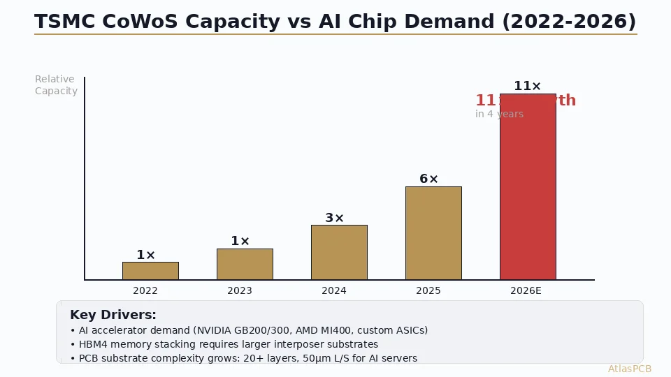
Modern AI accelerators (NVIDIA B200, AMD MI400, custom ASICs) use die sizes exceeding 800 mm². These massive dies are mounted on substrates using thousands of microbumps at 40-55 µm pitch. At these dimensions, even minimal substrate warpage causes:
- Bump non-contact: Warpage > 50 µm can prevent solder joints from forming during reflow
- Bridging: Adjacent bumps connect due to substrate bow
- Stress concentration: Uneven loading accelerates fatigue failure
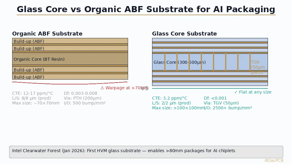
Organic substrates (BT resin, ABF build-up) typically exhibit 50-100 µm warpage on 50×50 mm panels after multi-layer lamination. Glass, by contrast, maintains < 10 µm warpage on the same panel size — a 5-10× improvement that enables reliable assembly of the largest dies currently in production.
CTE Matching to Silicon
The coefficient of thermal expansion (CTE) mismatch between substrate and die is the primary driver of solder joint fatigue in flip-chip packages:
| Material | CTE (ppm/°C) | Mismatch vs Silicon |
|---|---|---|
| Silicon die | 2.6 | — |
| Glass (borosilicate) | 3.2 | 0.6 (23%) |
| BT resin (organic) | 14 | 11.4 (438%) |
| ABF build-up | 17 | 14.4 (554%) |
| Copper | 17 | 14.4 (554%) |
The 0.6 ppm/°C mismatch between glass and silicon is dramatically less than the 11-14 ppm/°C gap with organic substrates. This translates directly to bump reliability: simulation models predict 3-5× improvement in thermal cycling lifetime for glass-based packages.
Dielectric Properties for High-Frequency Applications
Glass offers exceptional RF performance:
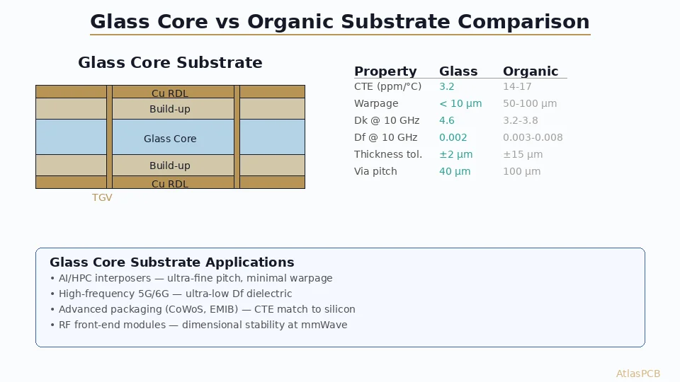
- Dk (dielectric constant): 4.6 for borosilicate glass — slightly higher than ultra-low-loss organic laminates (3.2-3.8), but with far better consistency
- Df (dissipation factor): 0.002 at 10 GHz — matching or exceeding the best organic materials (Megtron 7, Tachyon)
- Stability: Glass Dk/Df remain constant across temperature (-40°C to +150°C) and humidity variations, unlike organic materials that absorb moisture
For 5G mmWave and future 6G applications operating at 28-100 GHz, this stability is essential for maintaining filter response, antenna impedance matching, and transmission line characteristics.
Through Glass Via (TGV) Technology
Fabrication Methods
TGV formation is the critical enabling technology for glass core substrates. Three primary methods are used:
1. UV Laser Drilling
- Wavelength: 355 nm or 532 nm
- Via diameter: 30-100 µm
- Aspect ratio: Up to 10:1
- Best for: Moderate-density interconnects (100+ µm pitch)
- Advantages: High throughput, well-understood process
2. Laser-Induced Deep Etching (LIDE)
- Process: Femtosecond laser modifies glass structure, then selective HF etching removes modified material
- Via diameter: 10-50 µm
- Aspect ratio: Up to 20:1
- Best for: Ultra-fine pitch (< 80 µm)
- Advantages: Highest aspect ratio, smooth sidewalls
3. Electrochemical Discharge Machining (ECDM)
- Via diameter: 50-200 µm
- Aspect ratio: Up to 5:1
- Best for: Larger vias, power/ground connections
- Advantages: No thermal damage to surrounding glass, scalable to panel-level
TGV Metallization
After via formation, the glass holes must be metallized:
- Seed layer deposition: PVD Ti/Cu (30/300 nm) provides adhesion and initial conductivity
- Conformal copper plating: Electroplating fills the via (for smaller vias) or coats sidewalls (for larger vias)
- Fill strategy:
- Vias < 50 µm: Full copper fill using superfilling chemistry
- Vias 50-100 µm: Conformal coat + cap plating
- Vias > 100 µm: Conformal coat + paste fill + cap
Design Rules for TGV (Current State-of-Art)
| Parameter | Production Capability | Research Demonstrated |
|---|---|---|
| Via diameter | 50 µm | 10 µm |
| Via pitch | 80 µm | 40 µm |
| Aspect ratio | 8:1 | 20:1 |
| Via density | 1,500/cm² | 10,000/cm² |
| Registration accuracy | ±5 µm | ±2 µm |
| Glass thickness | 100-500 µm | 50 µm |
Advanced Substrate Manufacturing Support
AtlasPCB offers engineering consultation for next-generation substrate designs including HDI, UHDI, and advanced interposer layouts.
Discuss Your Project →Manufacturing Process Overview
Panel-Level Glass Processing
Unlike wafer-level processing (limited to 300 mm), glass substrates leverage panel-level manufacturing:
- Panel sizes: 510×515 mm or 600×600 mm (versus 300 mm wafer diameter)
- Throughput advantage: 3-5× more substrate units per panel compared to wafer processing
- Cost implication: Panel processing is key to making glass substrates cost-competitive with organic at scale
Process Flow
- Glass panel preparation: CNC scoring, cleaning, surface activation
- TGV formation: Laser drilling or LIDE processing
- Seed layer deposition: Sputtered Ti/Cu on both faces and via sidewalls
- Photolithography: Fine-line patterning (L/S 5/5 µm capable)
- Copper plating: Via fill + conductor formation
- Build-up layers: ABF or photoimageable dielectric lamination (similar to organic)
- Surface finish: ENIG, ENEPIG, or Cu-OSP depending on assembly method
- Singulation: Laser or mechanical dicing
Key Manufacturing Challenges
Glass breakage: Glass is brittle. Panel handling throughout the manufacturing line requires specialized carriers, edge protection, and stress-free clamping. Yield loss from cracking remains the #1 cost driver.
Chemical compatibility: Standard PCB wet processes (acidic/alkaline etching, cleaning) can attack certain glass compositions. Process chemistry must be validated for each glass type.
Thermal budget: While glass withstands higher temperatures than most organics, thermal shock from rapid heating/cooling can cause micro-cracking. Ramp rates during lamination and reflow must be carefully controlled.
Registration: The ultra-low CTE of glass means it expands less during thermal processing than organic substrates. Existing equipment calibrated for organic substrate expansion must be re-characterized for glass panels.
Application Domains
AI/HPC Interposers
The primary market driver. AI accelerator packages requiring 2.5D or 3D integration use glass interposers as alternatives to silicon interposers:
- CoWoS alternative: TSMC’s CoWoS uses expensive silicon interposers. Glass offers similar flatness at potentially lower cost for next-generation designs
- EMIB-like integration: Intel’s Embedded Multi-die Interconnect Bridge concept can leverage glass for the local interconnect bridge, offering better Dk/Df than silicon
5G/6G RF Front-End Modules
Glass substrates enable integration of RF filters, antenna arrays, and front-end modules:
- Consistent Dk enables precise filter frequency placement
- TGVs provide low-inductance ground connections for antenna elements
- Panel-level manufacturing suits the high-volume demands of 5G infrastructure
Automotive Radar and LiDAR
Autonomous driving sensors require substrates that maintain consistent electrical performance across automotive temperature ranges (-40°C to +150°C). Glass’s temperature-stable dielectric properties outperform organic materials in this application.
Photonics Integration
Emerging silicon photonics applications benefit from glass substrates:
- Optical waveguides can be directly formed in glass
- Low Df minimizes signal loss for RF portions of optical transceivers
- CTE matching prevents stress-induced birefringence in photonic elements
Cost and Market Outlook
SEMI’s May 2026 market report positions glass core substrates at an inflection point:
- Current pricing: 2-5× more expensive than equivalent organic substrates (per unit area)
- Cost reduction path: Panel-level processing at 600×600 mm is expected to achieve parity with high-end organic substrates (ABF build-up) by 2028
- Market size: $200M (2026) → $2B+ (2030 projected)
- Key players: Intel (Sustrate), Samsung (S-CORE), Corning, AGC, Schott
The cost premium is acceptable for applications where organic substrates physically cannot meet specifications — large interposers (> 2,500 mm²), ultra-fine pitch assembly (< 60 µm), and applications requiring < 20 µm total warpage.
Design Considerations for Engineers
Stackup Planning
Glass core substrates use a similar approach to traditional HDI — core + build-up layers:
Build-up L1: Fine-line RDL (5/5 µm L/S)
Build-up L2: Semi-fine (8/8 µm L/S)
Glass Core: 200 µm borosilicate with TGV
Build-up L3: Semi-fine (8/8 µm L/S)
Build-up L4: Fine-line RDL (5/5 µm L/S)
Total thickness: 300-500 µm typical for interposer applications.
Simulation Considerations
- Mechanical FEA: Use actual glass CTE (3.2 ppm/°C) and Young’s modulus (70 GPa vs 25 GPa for organic)
- Signal integrity: Glass Dk is higher than ultra-low-loss organics — account for this in impedance calculations
- Thermal: Glass thermal conductivity (1.0-1.2 W/m·K) is lower than FR-4 (0.3 W/m·K in-plane with copper layers). Thermal via arrays remain essential.
DFM Guidelines
- Minimum glass core thickness: 100 µm (thinner panels have handling issues)
- Keep TGV density balanced (top-heavy designs cause warpage during plating)
- Account for glass edge exclusion zone (5 mm from panel edge)
- Use stress-relief structures (rounded pad shapes, no 90° corners on RDL)
Further Reading
- Sequential Lamination vs Build-up HDI Process
- VIPPO Via-in-Pad Plated Over Design and Manufacturing
- PCB Via Size Selection Guide
- RF PCB Rogers vs PTFE Material Selection
Planning an advanced packaging project that requires glass core or ultra-fine-pitch substrates? Get in touch with our engineering team to discuss manufacturing feasibility and capabilities.
About AtlasPCB — We specialize in complex PCB manufacturing for HDI, RF, and high-reliability applications. Explore our RF and high-frequency PCB services . Every order includes free engineering review. Get your quote.
Reviewed by AtlasPCB Engineering Team — IPC-certified manufacturing specialists with 15+ years of production experience in HDI, RF, and high-reliability PCB fabrication. Content based on factory floor data and real customer design reviews.
- glass core substrate
- advanced packaging
- TGV
- through glass via
- interposer
- AI PCB
- CoWoS
- CTE matching
- RF substrate