· AtlasPCB Engineering · Engineering · 6 min read
Horizontal vs Vertical Electroplating for PCB: Uniformity, Throughput and HDI Capability
Compare horizontal and vertical electroplating processes for PCB manufacturing — understand how each method affects copper thickness uniformity, production throughput, thin-panel handling, and suitability for HDI and advanced substrates.
The choice between horizontal and vertical electroplating is one of the most consequential process decisions in PCB manufacturing. It influences copper uniformity, microvia filling quality, thin-panel capability, production throughput, and ultimately the board’s electrical performance. As designs push toward finer features and thinner substrates — driven by HDI, IC substrates, and advanced packaging — this decision increasingly determines whether a manufacturer can execute your design.
Understanding both approaches helps engineers specify realistic tolerances and select manufacturers whose process capabilities match their design requirements.
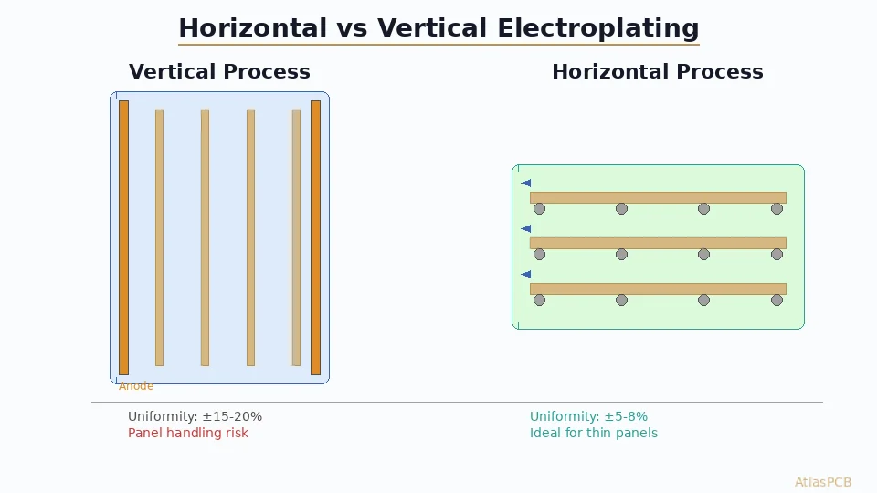
Vertical Electroplating: The Traditional Approach
How It Works
In vertical (rack or flight-bar) plating, PCB panels are:
- Clamped to metal flight bars at their top edge
- Lowered vertically into plating tanks
- Immersed in electrolyte solution (copper sulfate + sulfuric acid + additives)
- Connected as cathodes with anodes positioned on both sides of the tank
- Plated for a controlled time at specified current density
- Raised, rinsed, and transferred to subsequent process steps
The panels hang vertically in the solution, and copper deposits onto all exposed surfaces simultaneously.
Advantages of Vertical Plating
Flexibility: Multiple panel sizes and thicknesses can be processed in the same tank by adjusting flight bar spacing and current settings.
Lower capital cost: Tank-based systems require less investment than horizontal conveyorized lines for low-to-medium volume production.
Large panel capability: Panels up to 24” × 30” or larger can be processed in appropriately sized tanks.
Process visibility: Operators can visually inspect panels during processing, and individual panels can be pulled for inspection without stopping the line.
Limitations
Uniformity challenges: Current distribution varies with position:
- Panel edges receive higher current density (current crowding effect)
- Bottom areas may see different agitation vs. top
- Center panels in a loaded rack receive less current than outer panels
- Typical uniformity: ±15-20% across a single panel
Thin panel damage: Panels below 0.4mm bow under their own weight and can be damaged by flight bar clamps.
Throughput constraints: Batch processing with load/unload cycles limits throughput compared to continuous conveyorized lines.
Horizontal Electroplating: The Modern Standard for HDI
How It Works
In horizontal (conveyorized) plating:
- Panels enter the system flat on a roller conveyor
- They pass through successive zones: pre-clean, activate, plate, rinse
- Electrolyte is delivered via flood nozzles or submerged spray bars above and below the panel
- Insoluble anodes are positioned parallel to the panel surface at controlled, uniform distances
- Panels exit the system continuously at the other end
The panel never changes orientation — it remains flat throughout processing.
Advantages of Horizontal Plating
Superior uniformity: ±5-8% copper thickness uniformity across the entire panel because:
- Anode-to-cathode distance is constant (typically 10-15mm) across the full panel area
- Hydrodynamic conditions are uniform — electrolyte flows identically across all points
- No edge effects from rack position or current crowding at clamp points
Thin panel handling: Panels supported on rollers can be as thin as 0.05mm without bowing or mechanical damage. This is essential for:
- IC substrate manufacturing (50-100μm cores)
- Embedded component layers
- Flexible circuit plating
Continuous throughput: No load/unload cycles. Panels feed continuously, limited only by plating time (conveyor speed). Typical throughput: 2-4 panels/minute depending on plating thickness required.
Uniform microvia filling: The controlled hydrodynamics deliver fresh electrolyte into blind via cavities from both sides simultaneously, producing more uniform via fill with fewer center voids.
Limitations
Higher capital investment: A full horizontal plating line costs $2-5M versus $300K-800K for a comparable vertical system.
Panel size constraints: Conveyor width limits maximum panel dimension (typically ≤ 24” width).
Chemistry management: Higher flow rates consume additives faster, requiring more sophisticated replenishment control.
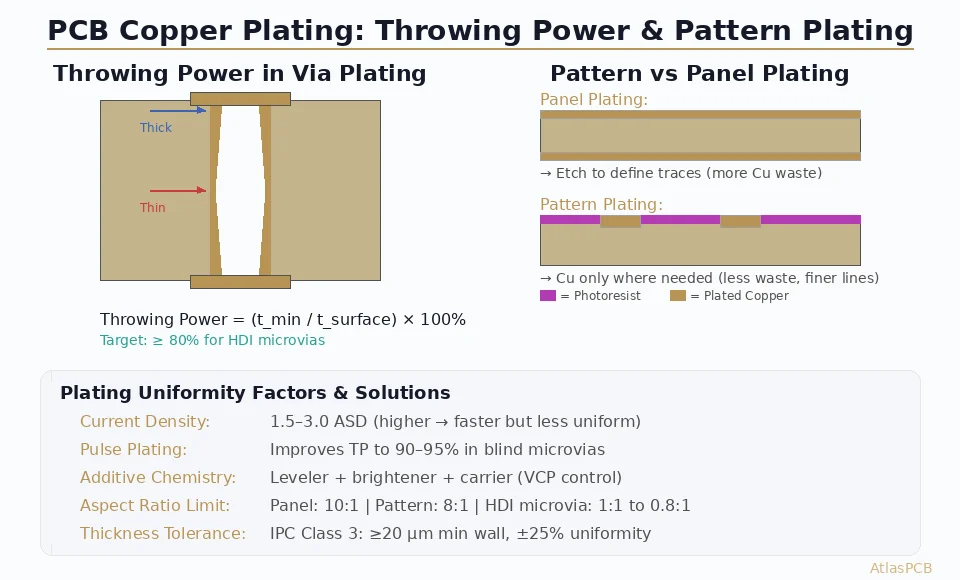
Technical Comparison
Copper Thickness Uniformity
| Parameter | Vertical | Horizontal |
|---|---|---|
| Panel uniformity | ±15-20% | ±5-8% |
| Hole-to-surface ratio | 60-80% | 80-95% |
| Edge vs. center variation | 25-40% difference | 5-10% difference |
| Panel-to-panel consistency | ±10-15% | ±3-5% |
For controlled impedance boards where trace thickness directly affects impedance, horizontal plating’s uniformity translates to tighter impedance tolerance at the same design rules.
View Our Process Capabilities → | Get a Quote
Microvia Fill Performance
Blind microvia filling quality depends heavily on electrolyte delivery into the via cavity:
Vertical: Electrolyte enters the via from one side (the open face). Convective transport is limited by tank agitation patterns. Result:
- Center dimple or void common in vias ≤ 100μm diameter
- Requires aggressive pulse-reverse waveforms to compensate
- Fill percentage typically 70-85% for aspect ratio > 0.8
Horizontal: Electrolyte contacts both panel faces simultaneously with controlled flow velocity. Result:
- More uniform deposition inside the via
- Fill percentage typically 85-95% for the same geometry
- Fewer center voids, more predictable cap plating flatness
Throwing Power in Through-Holes
For through-hole plating, the challenge is achieving adequate plating at the barrel center (maximum distance from the surface):
| Aspect Ratio | Vertical (center thickness vs. surface) | Horizontal |
|---|---|---|
| 5:1 | 60-70% | 75-85% |
| 8:1 | 45-60% | 65-75% |
| 10:1 | 35-50% | 55-65% |
| 12:1+ | Requires specialty process | 45-55% |
Production Economics
| Factor | Vertical | Horizontal |
|---|---|---|
| Capital cost | $300K-$800K | $2M-$5M |
| Floor space | Smaller footprint | 20-40m line length |
| Labor | Higher (manual handling) | Lower (automated) |
| Throughput | 30-60 panels/hour | 120-240 panels/hour |
| Chemistry consumption | Lower | Higher (fast flow) |
| Suitable volume | Low-medium | Medium-high |
When to Specify Horizontal Plating
Mandatory Applications
- HDI with microvias < 100μm: Uniform filling requires controlled hydrodynamics
- Panels < 0.4mm thick: Cannot be flight-bar hung without damage
- IC substrates and interposers: 50μm cores demand horizontal processing
- Fine line (< 50μm L/S): Thickness uniformity directly affects etching yield
- Controlled impedance ≤ ±5%: Cannot achieve with vertical plating uniformity
Preferred but Not Mandatory
- High-volume production (> 500 panels/day): Throughput economics favor horizontal
- Multi-layer boards > 12 layers: Uniformity compounding across layers
- Automotive/aerospace Class 3: Tighter plating specifications more easily met
Vertical Is Adequate For
- Standard 4-6 layer boards with ≥ 100μm features
- Prototype and low-volume production (< 50 panels/lot)
- Large format panels exceeding horizontal line width limits
- Flexible circuits on carriers (specialized rack mounting)
Process Control and Monitoring
Vertical System Monitoring
- Hull cell testing: Weekly assessment of additive balance
- Thickness mapping: Test coupon measurement at 5-9 points per panel
- Current distribution modeling: Finite element simulation for new panel layouts
- Anode maintenance: Bag replacement, geometry inspection
Horizontal System Monitoring
- In-line thickness gauging: X-ray fluorescence at multiple points, real-time feedback
- Flow rate monitoring: Ensure uniform electrolyte delivery across panel width
- Conveyor speed control: Directly determines plating thickness
- Additive dosing: Automated consumption-based replenishment with CVS analysis
Emerging Trends: Hybrid Approaches
Modern PCB factories increasingly use both systems:
- Panel plating (horizontal): Initial copper buildup for uniformity on thin cores
- Pattern plating (vertical): Selective plating through photoresist for final traces
This hybrid approach captures horizontal’s uniformity advantage for the critical base copper while using vertical’s flexibility for pattern-specific plating where absolute uniformity matters less.
Pulse and Pulse-Reverse Plating
Both systems benefit from advanced waveform control:
- Forward pulse: Deposits copper in controlled bursts
- Reverse pulse: Partially dissolves high-current-density areas (edges, corners)
- Net effect: Improved uniformity and via filling in both orientations
Further Reading
- PCB Copper Plating Thickness Uniformity: Electroless vs Electrolytic Processes
- Sequential Lamination vs Buildup HDI Process
- HDI Microvia Stacked vs Staggered Reliability
Conclusion
The vertical-to-horizontal transition in electroplating mirrors the broader evolution of PCB manufacturing from craft-scale batch processing to precision continuous manufacturing. As designs shrink features, thin substrates, and demand tighter tolerances, horizontal plating’s inherent uniformity advantages become decisive.
For engineers designing high-density boards: ask your manufacturer which plating orientation they’ll use for your job. If your design has microvias below 100μm, controlled impedance below ±5% tolerance, or substrate thickness below 0.4mm, horizontal plating isn’t a nice-to-have — it’s a manufacturing requirement.
Need precision HDI with horizontal plating uniformity? AtlasPCB’s conveyorized plating lines handle substrates from 0.1mm to 3.2mm with documented ±7% thickness uniformity. Request a quote →
About AtlasPCB — We specialize in complex PCB manufacturing for HDI, RF, and high-reliability applications. Explore our HDI PCB manufacturing capabilities, or get an full PCB manufacturing capabilities . Every order includes free engineering review. Get your quote.
Reviewed by AtlasPCB Engineering Team — IPC-certified manufacturing specialists with 15+ years of production experience in HDI, RF, and high-reliability PCB fabrication. Content based on factory floor data and real customer design reviews.
- electroplating
- PCB manufacturing
- copper plating
- HDI
- process engineering
- uniformity