· AtlasPCB Engineering · Engineering · 7 min read
Eye Diagram Interpretation for PCB Signal Integrity: Jitter, ISI and Channel Loss Analysis
Learn to interpret eye diagrams for high-speed PCB signal integrity — understand eye height, eye width, jitter components, inter-symbol interference (ISI), and how PCB design choices affect 10-56 Gbps channel performance.
The eye diagram is the single most powerful visualization tool in high-speed PCB signal integrity. It compresses thousands of bit transitions into one image that immediately reveals whether your channel design will work at the target data rate — or whether loss, reflections, crosstalk, and jitter have consumed your margins until reliable communication becomes impossible.
For PCB designers working at 10 Gbps and above, learning to read eye diagrams isn’t just about post-silicon validation. It’s about understanding how your material selection, stackup design, via structure, and routing topology will affect the eye long before you commit to fabrication. Pre-layout simulation produces predicted eye diagrams; post-fabrication measurement confirms them.
Eye Diagram Fundamentals
How an Eye Diagram Is Constructed
An eye diagram is created by:
- Triggering an oscilloscope on the clock or data rate period
- Overlaying successive unit intervals (UIs) of the serial data stream
- Accumulating many transitions until a statistical pattern emerges
Each trace represents one bit period. Where traces cluster together, the signal is deterministic. Where they spread apart, uncertainty (jitter, noise) exists.
Anatomy of the Eye
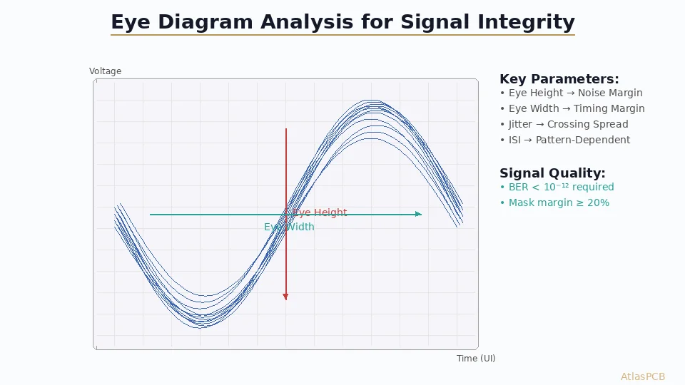
The resulting shape reveals key parameters:
Eye Height: The vertical opening at the center sampling point — represents available noise margin. Larger eye height means the receiver can tolerate more noise before making errors.
Eye Width: The horizontal opening — represents available timing margin. Wider means the receiver’s clock recovery has more tolerance for sampling position uncertainty.
Crossing Points: Where rising and falling transitions intersect — spread in crossing points indicates jitter. Tight crossings mean low jitter; wide spread means significant timing uncertainty.
Eye Closure: The difference between the ideal (zero-loss) eye and the actual measured eye — quantifies total channel degradation.
Jitter Components Visible in the Eye
Deterministic Jitter (DJ)
Bounded, repeatable timing variations:
- ISI (Inter-Symbol Interference): Pattern-dependent — previous bits affect current bit timing through dispersion. Visible as trace-to-trace position variation.
- Duty Cycle Distortion (DCD): Asymmetry between rise and fall times. Visible as unequal crossing heights.
- Periodic Jitter (PJ): Coupled interference from clock harmonics, switching regulators, or crosstalk. Visible as modulated crossing positions.
- Bounded Uncorrelated Jitter (BUJ): Simultaneous switching noise, crosstalk from random data on adjacent pairs.
Random Jitter (RJ)
Unbounded Gaussian distribution from thermal noise, shot noise in active devices, and phase noise in clock circuits. Contributes to BER through the tail of the Gaussian distribution:
BER = erfc(Q/√2) where Q = (Eye Height/2) / σ_noise
For BER = 10⁻¹²: Q ≈ 7, meaning eye height must be ≈14σ of combined noise.
Total Jitter Budgeting
Total Jitter (TJ) at a given BER:
TJ@BER = DJ + 2 × N(BER) × RJ_rms
Where N(10⁻¹²) ≈ 14.07
PCB designer impact: Most DJ comes from channel characteristics you control — impedance discontinuities, via transitions, trace length mismatches in differential pairs.
PCB Design Parameters That Affect the Eye
Dielectric Loss (Df)
The dominant eye-closure mechanism for traces longer than 3 inches above 10 Gbps:
| Material | Df @10GHz | Max Trace Length @25Gbps (open eye) |
|---|---|---|
| Standard FR-4 | 0.020 | ~3 inches |
| Mid-loss (Megtron 4) | 0.008 | ~8 inches |
| Low-loss (Megtron 7) | 0.004 | ~14 inches |
| Ultra-low-loss (Tachyon) | 0.002 | ~20+ inches |
Eye effect: High Df attenuates Nyquist frequency components, rounding edges and reducing eye height. This is the primary cause of ISI-induced eye closure.
Impedance Discontinuities
Every impedance mismatch creates reflections that arrive at the receiver as ghost signals, closing the eye:
- Via transitions: Typical via stub adds 3-5% eye closure per transition at 25 Gbps
- Connector interfaces: Launch parasitics can add 10-20% eye closure without optimization
- Reference plane gaps: Current return path disruption creates radiation and reflection
Request SI-Optimized Quote → | Engineering Services
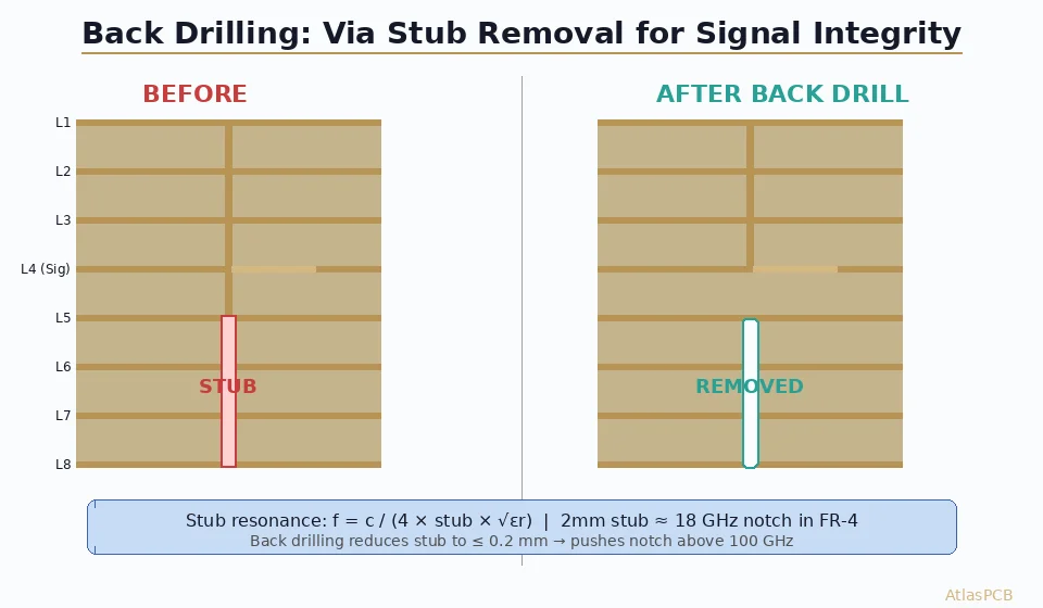
Via Stub Resonance
Unterminated via stubs act as quarter-wave resonators that create notches in the channel transfer function:
f_notch = c / (4 × L_stub × √εr)
At 25 Gbps with 60-mil stub length in FR-4: f_notch ≈ 12 GHz — right at the Nyquist frequency, severely closing the eye.
Solution: Back-drilling removes the unused stub portion, recovering 5-15 dB of insertion loss at the notch frequency and significantly reopening the eye.
Differential Pair Skew
Intra-pair length mismatch converts differential signal energy to common-mode:
- 5 mil skew at 25 Gbps: ~2% eye height reduction
- 20 mil skew at 25 Gbps: ~8% eye height reduction, mode conversion warning
- 50+ mil skew at 56 Gbps PAM4: Potential compliance failure
Crosstalk
Near-end (NEXT) and far-end (FEXT) coupling from adjacent pairs:
- Appears as noise on the eye diagram, reducing effective eye height
- Rule of thumb: maintain ≥3× dielectric height spacing between differential pairs
- Each pair contributing 2-3% eye closure; 4 aggressors can consume 10% margin
Eye Diagram Measurement in Practice
Required Equipment
- Real-time oscilloscope: 33+ GHz bandwidth for 25 Gbps NRZ, 50+ GHz for 56 Gbps PAM4
- PRBS pattern generator: PRBS-31 or PRBS-23 for ISI characterization
- Calibrated test fixtures: De-embedding of connector and probe parasitics
- Compliance software: Automated mask testing per IEEE 802.3 or OIF-CEI specifications
Measurement vs. Simulation Correlation
Good correlation requires:
- Accurate material characterization (Dk/Df vs. frequency from actual laminate lot)
- Via modeling that captures all parasitic elements (stub, anti-pad, pad capacitance)
- Connector S-parameter models from vendor (not generic models)
- Surface roughness effects included (Hammerstad or Huray model)
Typical correlation target: eye height within ±15%, eye width within ±10% of measurement.
Statistical Eye vs. Oscilloscope Eye
Oscilloscope eye: Limited by acquisition depth (millions of UIs). Sufficient for DJ characterization but may not capture rare RJ events.
Statistical eye: Computed from channel S-parameters and jitter/noise probability distributions. Extrapolates to BER floors (10⁻¹² to 10⁻¹⁵) that would require days of real-time measurement.
For PCB design decisions, statistical eye analysis from simulation is more practical and provides BER contours directly.
Eye Diagram Improvement Techniques
Passive Channel Optimization (PCB Design)
- Material upgrade: Move to lower-Df laminate (biggest single improvement)
- Stub removal: Back-drill or use blind vias to eliminate resonances
- Impedance matching: Optimize via anti-pad for smooth transition
- Trace shortening: Reduce channel length where topology allows
- Pair spacing: Increase to reduce crosstalk budget consumption
Active Equalization (Chip-Level)
When passive optimization hits limits:
- TX de-emphasis: Pre-distort signal to compensate for channel loss
- CTLE (Continuous Time Linear Equalizer): Analog high-frequency boost at receiver
- DFE (Decision Feedback Equalizer): Digital post-cursor ISI cancellation
- FEC (Forward Error Correction): Accept some eye closure, correct errors in digital domain
Modern 56 Gbps PAM4 links use all four techniques simultaneously. The PCB designer’s job is ensuring the channel loss stays within the equalization capability range.
PAM4 Eye Diagrams: Three Eyes, New Challenges
For 56+ Gbps PAM4 signaling, the eye diagram shows three vertically stacked eyes:
- Upper eye: Transition between levels 2→3
- Middle eye: Transition between levels 1→2
- Lower eye: Transition between levels 0→1
Each eye is approximately 1/3 the height of an NRZ eye at the same voltage swing, making PAM4 dramatically more sensitive to:
- Linearity (non-equal eye heights indicate compression)
- Noise (3× tighter noise margin per eye)
- ISI (pattern-dependent effects amplified by four levels)
PCB implications: PAM4 interfaces demand the lowest-loss materials, shortest possible trace lengths, and most aggressive via optimization to maintain adequate opening in all three eyes.
Further Reading
- Microstrip vs Stripline: Signal Integrity Comparison
- Differential Pair Routing: Tight vs Loose Coupling
- PCB Back-Drilling Via Stub Removal for Signal Integrity
Conclusion
Eye diagrams translate complex frequency-domain channel behavior into an intuitive visualization that directly correlates with bit error rate. For PCB designers, every routing decision, material selection, and via structure choice manifests in the eye — either keeping it open or closing it toward the BER cliff.
Master eye diagram interpretation to predict design success before fabrication, communicate effectively with signal integrity teams, and make informed trade-offs between cost (standard FR-4, no back-drilling) and performance (ultra-low-loss materials, optimized via transitions).
Designing 25+ Gbps interfaces and need a PCB partner with SI expertise? AtlasPCB provides impedance-controlled fabrication with Megtron 6/7, precision back-drilling (±2 mil depth control), and pre-production SI simulation support. Get a quote →
About AtlasPCB — We specialize in complex PCB manufacturing for HDI, RF, and high-reliability applications. Explore our impedance-controlled PCB manufacturing . Every order includes free engineering review. Get your quote.
Reviewed by AtlasPCB Engineering Team — IPC-certified manufacturing specialists with 15+ years of production experience in HDI, RF, and high-reliability PCB fabrication. Content based on factory floor data and real customer design reviews.
- signal integrity
- eye diagram
- jitter
- high-speed design
- channel loss
- ISI