· AtlasPCB Engineering · Engineering · 8 min read
AI-Powered EDA Tools in 2026: How Autonomous Agents Are Reshaping PCB Design from Schematic to Fabrication
Explore how AI-powered EDA tools from Siemens Fuse, Quilter, Flux, and Cadence are transforming PCB design in 2026. Learn how autonomous AI agents handle placement, routing, DFM verification, and signal integrity analysis — and what this means for hardware engineers and PCB manufacturers.
Introduction: The AI Revolution in Electronic Design Automation
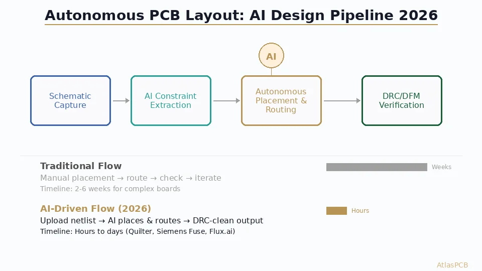
The printed circuit board design process has remained fundamentally manual since the transition from tape-based layout to CAD tools in the 1990s. While EDA software automated drafting and introduced design rule checks, the core intellectual work — component placement, routing strategy, stackup optimization, and signal integrity verification — remained firmly in human hands for three decades.
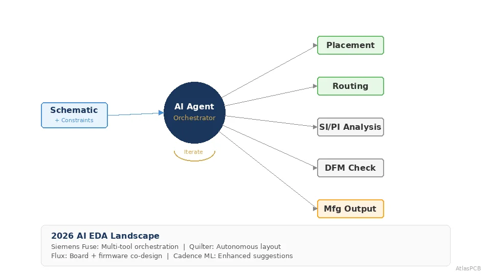
In 2026, that paradigm is definitively changing. A new generation of AI-powered tools has moved beyond autocomplete-style suggestions to autonomous execution of complete design workflows. From Siemens’ Fuse EDA AI Agent orchestrating multi-tool semiconductor and PCB processes, to Quilter delivering fully autonomous PCB layout, to Flux automating board and firmware development simultaneously — the industry is witnessing the emergence of AI agents that don’t just assist designers but replace entire phases of the design cycle.
This article examines the current state of AI in PCB EDA, compares the major platforms, analyzes their strengths and limitations, and explores what autonomous design means for hardware engineers and PCB manufacturers.
The Evolution: From Autorouter to Autonomous Agent
Generation 1: Pattern-Based Autorouters (1990s–2010s)
Early autorouters used maze-solving algorithms (Lee’s algorithm, A* pathfinding) to connect net endpoints while avoiding obstacles. They worked for simple designs but produced suboptimal results on complex boards — messy routing, poor impedance control, and designs that needed extensive manual cleanup.
Capability: Route connectivity. Quality: 40–60% of a skilled engineer.
Generation 2: Constraint-Driven Tools (2010s–2023)
Modern EDA platforms (Altium Designer, Cadence Allegro, Mentor Xpedition) added constraint managers that encode design rules — impedance targets, length matching, spacing requirements — and routers that respect these constraints. Interactive routing with real-time DRC checking became standard.
Capability: Constraint-compliant routing. Quality: 70–85% of a skilled engineer.
Generation 3: ML-Enhanced Assistance (2023–2025)
Machine learning entered EDA as suggestion engines: recommending component placements based on pattern recognition from successful designs, predicting signal integrity issues before simulation, and auto-fixing common DRC violations.
Capability: Intelligent suggestions + automated fixes. Quality: 85–95% on specific tasks.
Generation 4: Autonomous Agents (2025–Present)
The current generation operates as autonomous agents — systems that plan, execute, verify, and iterate through complete design workflows without human intervention for routine tasks. They combine domain-specific AI models with traditional physics-based verification tools.
Capability: End-to-end workflow execution. Quality: 90–98% on well-constrained problems.
Major AI EDA Platforms in 2026
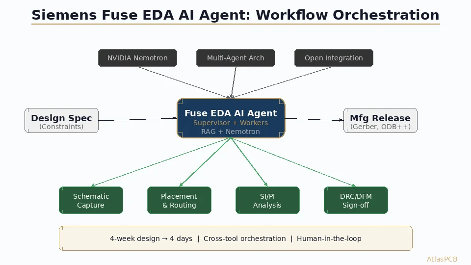
Siemens Fuse EDA AI Agent
Launched: March 2026 Approach: Multi-tool workflow orchestration
Siemens’ Fuse EDA AI Agent is the most ambitious deployment of autonomous AI in the EDA space. Rather than building a new design tool, Siemens created an AI orchestration layer that coordinates existing best-in-class tools:
- Xpedition for PCB layout and routing
- HyperLynx for signal and power integrity
- Calibre for physical verification and DFM
- Tessent for design-for-test
- Innovator3D IC for advanced packaging
The agent plans execution strategies, passes results between tools, interprets outputs, and iterates until constraints are met — mimicking the workflow of a senior engineer coordinating across multiple specialties.
Key differentiator: Cross-tool orchestration. No other platform spans from schematic through manufacturing sign-off with a single AI coordinator.
Limitation: Requires Siemens’ full EDA portfolio. Not tool-agnostic.
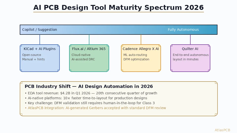
Quilter — Fully Autonomous PCB Layout
Status: Production-ready for 4–12 layer designs Approach: Physics-driven autonomous design from netlist
Quilter takes the most radical approach: upload a schematic/netlist and constraints, and the system produces a complete DRC-clean PCB layout — placement, routing, copper pours, and manufacturing outputs — without human interaction.
The “Project Speedrun” demonstration showed Quilter designing a complete computer (Arm-based SBC with DDR4, PCIe, USB, Ethernet) from schematic to fabrication-ready files, with the resulting hardware successfully booting and running real workloads.
Key differentiator: Zero human interaction for routine designs. Fastest time-to-layout.
Limitation: Less control over aesthetic preferences and non-quantifiable engineering judgment. Best suited for designs where optimal is measurably definable (impedance, thermal, DFM compliance).
Flux — AI-Driven Board + Firmware Development
Funding: $37 million (Series B led by 8VC, February 2026) Approach: Combined PCB layout and firmware automation
Flux uniquely combines hardware design with firmware generation, addressing the full embedded system development workflow:
- Schematic capture with AI-suggested topologies
- Board layout with automated placement and routing
- Bill-of-materials optimization based on availability and cost
- Firmware scaffolding from hardware pin mapping
CEO Matthias Wagner’s vision: reduce hardware development costs to near-zero so that “anyone can develop PCBs more easily.”
Key differentiator: Software + hardware co-design. Non-specialists can create working embedded systems.
Limitation: Less suitable for high-performance designs requiring deep domain expertise (RF, power electronics, high-speed SerDes).
Cadence ML-Enhanced Allegro/OrCAD
Approach: ML optimization within traditional workflow
Cadence takes an incremental approach: enhancing Allegro’s existing workflow with ML models for specific tasks:
- Placement optimization using reinforcement learning
- Routing guidance based on pattern recognition from successful designs
- Parasitic prediction without full extraction
- Auto-tuning of constraint values based on simulation goals
Key differentiator: Familiar workflow enhanced rather than replaced. Lowest adoption barrier.
Limitation: Still fundamentally human-driven. AI assists rather than executes.
Designing with AI EDA Tools? We Ensure Manufacturability.
AtlasPCB's DFM review catches issues that AI tools miss at manufacturing boundaries. Get expert feedback before committing to fabrication.
Request DFM Review →What AI Handles Well vs. Where Humans Remain Essential
AI Excels At:
Placement optimization:
- Minimizing total interconnect length across 500+ components
- Grouping by function (power, digital, analog, RF) with appropriate separation
- Thermal placement considering power dissipation and airflow
- Manufacturing-aware placement (component orientation, fiducial access, test point accessibility)
Routing execution:
- Differential pair routing with matched lengths within 1 ps skew
- Power delivery network design with optimal decoupling capacitor placement
- Fan-out routing for fine-pitch BGAs (0.4–0.65 mm pitch)
- Via optimization for layer transitions (minimizing stub length, impedance discontinuity)
Verification and iteration:
- Running full DRC suites and auto-fixing violations
- Impedance checking against targets with automatic geometry adjustment
- Timing analysis and length-matching optimization
- Repetitive constraint verification across thousands of nets
Humans Remain Essential For:
Architecture decisions:
- Choosing between microstrip and stripline for specific signal groups
- Selecting materials for novel applications (new low-loss laminates, metal-core substrates)
- Defining thermal management strategy (embedded cooling, thermal via arrays, heatsink attachment)
- Making cost/performance trade-offs specific to product requirements
Manufacturing risk assessment:
- Evaluating whether an AI-generated design pushes fabrication capabilities beyond reliable yield
- Understanding factory-specific process variations that aren’t captured in standard design rules
- Assessing mechanical reliability for specific operating environments (thermal cycling, vibration, humidity)
Novel physics problems:
- First-time designs with untested material combinations
- Edge cases where simulation models lack validation data
- Interference patterns specific to product enclosures and mechanical assemblies
Impact on PCB Manufacturing
What Manufacturers See From AI-Designed Boards
As AI tools proliferate, PCB fabricators report characteristic patterns in AI-generated designs:
- Tighter feature utilization: AI pushes to process minimums (3/3 mil line/space when capability is 3/3, rather than conservative 4/4 mil with margin)
- More complex via structures: AI optimizes signal paths through whatever via technology is available, resulting in designs with mixed via types (through, blind, buried, stacked microvias)
- Thinner dielectrics: AI targets impedance through geometry optimization, often selecting thinner prepreg than human designers would default to
- Higher layer counts: AI’s ability to handle complexity reduces reluctance to add layers for signal integrity improvement
- Better DFM compliance on basics: Fewer acid traps, proper annular rings, correct thermal relief patterns
Manufacturing Capability Requirements
To serve AI-designed PCBs, fabricators need:
- LDI (Laser Direct Imaging): 25 μm line/space capability for fine-feature designs
- Sequential lamination: HDI builds with multiple drill-laminate cycles
- Precision impedance control: ±5% tolerance (vs. industry-standard ±10%)
- Advanced materials: Low-loss laminates (Megtron 6, Tachyon, IS680) for AI-optimized high-speed designs
- DFM feedback integration: API-accessible design rule databases that AI tools can query
The Statistics: AI Adoption in PCB Design
Industry surveys and market data paint a picture of rapid adoption:
- AI PCB market size: $5.6 billion in 2025, projected $10 billion in 2026 (including AI-demand PCBs and AI design tools)
- Adoption rate: 45% of PCB design teams using some form of AI assistance in 2026 (up from 15% in 2024)
- Productivity impact: Teams report 2–5× improvement in time-to-first-article for routine designs
- Quality impact: 30–50% reduction in DRC violations reaching fabrication
- Skill gap concern: Only 19% of small PCB firms have AI-skilled talent for tool deployment
Practical Recommendations for Hardware Teams
Getting Started with AI EDA
- Start with constrained problems: Use AI routing for well-defined signal groups (DDR, PCIe, USB) where constraints are explicit and measurable
- Validate with traditional tools: Run standard SI/PI simulations on AI-generated designs before committing to fabrication
- Maintain DFM communication: Share your fabricator’s actual process capabilities with AI tools (not just standard IPC minimums)
- Build comparison data: Run parallel designs (human vs. AI) on the same requirements to quantify quality and time differences
- Invest in verification skills: As AI handles more execution, engineer value shifts toward specification quality and verification rigor
Fabricator Selection for AI-Generated Designs
When choosing a PCB manufacturer for boards designed with AI tools:
- Verify advanced capability (HDI, fine-line, tight impedance) since AI designs often use process limits
- Confirm DFM review services that catch manufacturing risks AI tools might miss
- Ensure engineering communication — AI-designed boards may need fabricator input on material substitutions or process adjustments
- Request first-article TDR data to validate AI-predicted impedance matches fabricated reality
Further Reading
- [PCB Laser Direct Imaging (LDI) vs. Phototool Lithography]/blog/pcb-laser-direct-imaging-ldi-vs-phototool/) — The imaging technology enabling AI-pushed fine features
- [Controlled Impedance PCB Design and Stackup]/blog/controlled-impedance-pcb-design-stackup-calculations/) — Foundation for AI impedance optimization
- [HDI Microvia: Stacked vs. Staggered Reliability]/blog/hdi-microvia-stacked-vs-staggered-reliability/) — Via technologies AI tools leverage
- [Differential Impedance for PCIe Gen5 and DDR5]/blog/differential-impedance-pcie-gen5-ddr5-microstrip-stripline/) — High-speed constraints AI agents must satisfy
Conclusion
AI-powered EDA tools in 2026 represent a genuine paradigm shift in PCB design methodology. The transition from human-executed, tool-assisted design to AI-executed, human-supervised design is well underway for routine designs. Siemens’ cross-tool orchestration, Quilter’s autonomous layout, and Flux’s combined hardware-software automation each address different segments of the design spectrum.
For hardware engineers, the optimal strategy is embracing AI for execution efficiency while strengthening skills in architecture, specification, and verification — the areas where human judgment remains irreplaceable. For PCB manufacturers, preparing advanced fabrication capabilities and maintaining robust DFM communication channels positions them to serve the increasingly complex designs that AI tools enable.
Need manufacturing support for AI-designed PCBs? Contact AtlasPCB Engineering for a DFM review that validates your design against real-world process capabilities.
About AtlasPCB — We specialize in complex PCB manufacturing for HDI, RF, and high-reliability applications. Explore our impedance-controlled PCB manufacturing, or get an free engineering DFM review . Every order includes free engineering review. Get your quote.
Reviewed by AtlasPCB Engineering Team — IPC-certified manufacturing specialists with 15+ years of production experience in HDI, RF, and high-reliability PCB fabrication. Content based on factory floor data and real customer design reviews.
- AI
- PCB design
- EDA tools
- machine learning
- Siemens Fuse
- Quilter
- Flux
- autonomous design
- DFM
- signal integrity
- hardware engineering