· Engineering · 7 min read
How to Specify Via-in-Pad: DFM Requirements, Fill Options, and Common Mistakes
Complete DFM guide for specifying via-in-pad (VIP) in your PCB design. Covers fill types (conductive vs non-conductive), plating requirements, IPC-4761 classifications, Gerber annotation, and the fabrication constraints that determine cost and yield.
Quick Reference: Via-in-Pad Specification Checklist
Before submitting your design for fabrication, confirm these items in your fab drawing:
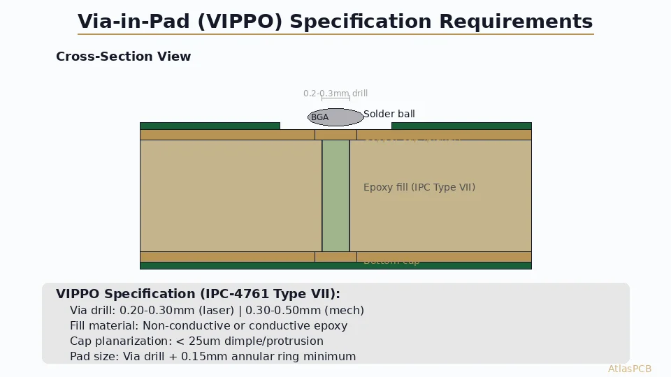
- Via drill size specified (typical: 0.1-0.3mm for VIP)
- Fill material called out (non-conductive epoxy or conductive)
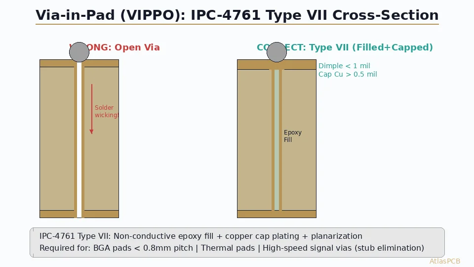
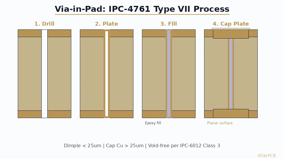
- IPC-4761 classification stated (Type VII = filled + capped)
- Maximum dimple depth specified (standard: < 25 um)
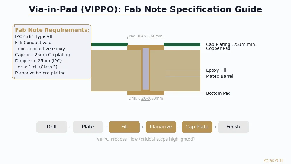
- Cap plating thickness noted (minimum 25 um copper)
- VIP vias identified on drill drawing or dedicated layer
- Annular ring adequate for cap plating (minimum pad diameter = drill + 0.15mm)
Why Via-in-Pad: The Routing Problem It Solves
Standard BGA fanout uses “dog-bone” routing: a short trace from the BGA pad to an adjacent via. This works for 1.0mm and 0.8mm pitch BGAs where there’s room between pads for the via and its annular ring.
At 0.5mm pitch and below, dog-bone fanout becomes impossible for inner ball rows. The via pad diameter plus clearance exceeds the available space between BGA lands. Via-in-pad eliminates this constraint by placing the via directly in the component pad.
When via-in-pad is required:
- BGA pitch <= 0.5mm (inner rows cannot escape with dog-bone)
- QFN/DFN exposed thermal pad (thermal vias directly under the pad)
- High pin-count BGAs (> 500 pins) at 0.65-0.8mm pitch (inner rows)
- RF designs requiring minimal stub length on signal transitions
When via-in-pad is optional but beneficial:
- BGA pitch 0.8mm where you want to recover routing channels
- Designs requiring maximum component density
- High-speed designs where via stub elimination matters
For a deeper look at BGA fanout strategies, see our guide on BGA fanout routing: dog-bone vs via-in-pad approaches.
IPC-4761 Via Fill Classifications
IPC-4761 defines seven types of via protection. For via-in-pad under BGA, you need Type VII:
| Type | Description | Use Case |
|---|---|---|
| I | Tented (dry film/solder mask) | Non-critical vias, low cost |
| II | Tented and covered | Slightly better than Type I |
| III | Plugged (solder mask or epoxy, not planar) | Vias not under pads |
| IV | Plugged and covered | Improved sealing |
| V | Filled (non-planar) | Vias not under components |
| VI | Filled and covered (not planar enough for BGA) | Thermal vias |
| VII | Filled and capped (planarized) | Via-in-pad under BGA |
Type VII process flow:
- Drill via (mechanical or laser)
- Plate through-hole copper (electroless + electrolytic, 20-25 um)
- Fill via with epoxy (vacuum or screen print)
- Cure epoxy (thermal oven, 150-180C)
- Planarize surface (ceramic brush or belt sander)
- Cap plate additional copper (25+ um over filled via)
- Final surface is flush with surrounding copper
HDI FABRICATION EXPERTISE
Via-in-Pad Done Right, First Time
AtlasPCB processes via-in-pad with both conductive and non-conductive fill on HDI boards up to 5+N+5 buildup. Laser vias down to 75um, cap plating verified by cross-section.
Upload Your BGA Design ›Fill Material Selection: Conductive vs Non-Conductive
Non-Conductive Epoxy Fill (Standard)
- Composition: Silica-filled epoxy resin
- CTE: 30-50 ppm/C (higher than copper, but constrained by barrel plating)
- Thermal conductivity: 0.5-1.0 W/mK (poor — not a thermal path)
- Cost: Standard — included in typical VIP process quote
- When to use: Signal vias under BGA, vias where only the barrel carries current
Conductive Fill (Copper or Silver Epoxy)
- Composition: Copper or silver particles in epoxy matrix
- Thermal conductivity: 3-15 W/mK (varies widely by product)
- Electrical resistance: Low but higher than solid copper
- Cost: 20-40% premium over non-conductive
- When to use: Thermal vias under QFN exposed pads, power vias carrying >1A per via
Common mistake: Specifying conductive fill for all vias “just in case.” This adds unnecessary cost. Only thermal vias and high-current power vias benefit from conductive fill. Signal VIP vias should use non-conductive fill.
Common DFM Mistakes and How to Avoid Them
Mistake 1: Insufficient Annular Ring for Cap Plating
After via fill and planarization, the fabricator must plate additional copper over the filled via. If your pad diameter doesn’t account for drill tolerance plus cap plating registration, the cap may not fully cover the fill material.
Rule: Minimum pad diameter = Drill diameter + 0.15mm (for mechanical drill) or + 0.10mm (for laser drill)
Example for 0.5mm pitch BGA:
- Pad diameter: 0.275mm (per IPC-7351)
- Maximum via drill: 0.275 - 0.15 = 0.125mm (laser via territory)
- If using mechanical drill (min 0.15mm): pad must be >= 0.30mm
Mistake 2: No VIP Callout in Fab Data
Placing a via on a pad in Altium, KiCad, or Cadence does not automatically communicate fill requirements to the fabricator. You must:
- Add a fab note: “All vias within BGA pad boundaries shall be filled and capped per IPC-4761 Type VII”
- OR create a dedicated drill layer for VIP vias (e.g., “Drill-VIP”)
- OR annotate specific vias in your drill chart
Without explicit instructions, the fabricator may deliver vias that are tented (solder mask only) or plugged (non-planar) — both cause solder voiding under BGA.
Mistake 3: Dimple Depth Not Specified
If you don’t specify maximum dimple, you may receive boards with 50-75 um concavity at the via center. This creates:
- Uneven solder paste deposition (reduced paste volume at via center)
- Solder voiding under BGA balls aligned with vias
- Potential tombstoning on small passives if via is partially under pad
Specify: “Maximum dimple/concavity at filled via surface: 25 um (1 mil) per IPC-4761 Type VII”
Mistake 4: Via Size Too Large for Reliable Fill
Mechanical vias larger than 0.35mm diameter are difficult to fill without voids. Larger vias trap air during the filling process, creating bubbles that expand during reflow and may crack the fill or cap plating.
Guidelines:
- Laser via (0.075-0.15mm): Fill is reliable and fast
- Small mechanical via (0.15-0.25mm): Standard fill process, high yield
- Medium mechanical via (0.25-0.35mm): Requires careful process control
- Large mechanical via (>0.35mm): Avoid for VIP — use plugging or resin fill only
DFM REVIEW INCLUDED
Catch These Issues Before Fabrication
Our engineering team checks your VIP specifications against our process capabilities during quoting. Annular ring violations, fill compatibility, and drill-to-pad alignment are flagged before production starts.
Submit Design for Review ›Fab Drawing Specification Template
Include this block (modified for your design) in your fabrication drawing:
VIA-IN-PAD REQUIREMENTS:
- Classification: IPC-4761 Type VII (Filled and Capped)
- Fill material: Non-conductive epoxy [or: Conductive copper epoxy]
- Applicable vias: [All vias within BGA U1-U5 pad boundaries]
  [or: All vias on drill layer "VIP-DRILL"]
- Maximum dimple (concavity): 25 um (1.0 mil)
- Maximum protrusion (convexity): 25 um (1.0 mil)
- Minimum cap plating thickness: 25 um
- Via fill shall be void-free per IPC-6012 Class 3 Section 3.6.2.11
- Cross-section verification: [required for first article / not required]
CAD Tool Setup Tips
Altium Designer: Create a separate drill pair for VIP vias. Set padstack to include “Plugged” property. Add manufacturing note linked to via class.
KiCad: Use drill layer assignment in custom rules. Add VIP note to User.Comments layer at board edge.
Cadence Allegro: Define VIP padstacks with explicit fill property. Use constraint region to identify VIP zones in fab documentation.
Cost Impact and Optimization Strategies
Via-in-pad adds process steps (fill, cure, planarize, cap plate) that increase cost:
| Board Type | VIP Cost Adder | Strategy |
|---|---|---|
| 4-layer, <50 VIP vias | +15-20% | Standard quoting |
| 6-layer HDI, 100-300 VIP vias | +20-30% | Combine with HDI pricing |
| 8+ layer, full VIP design | +25-35% | Negotiate volume pricing |
Cost optimization approaches:
- Use VIP only where required (inner BGA rows), use dog-bone for outer rows
- Standardize via size to reduce drill tool changes
- Specify non-conductive fill unless thermal requirements dictate otherwise
- Combine VIP fabrication with HDI process (laser vias are filled as part of sequential lamination)
For detailed HDI pricing considerations, see our HDI PCB cost breakdown and optimization guide.
VIA-IN-PAD CAPABILITIES
Laser Vias Down to 75um, Filled and Capped
Stacked microvias, staggered HDI, and mechanical VIP — all with IPC-4761 Type VII fill. Aspect ratios up to 16:1. Cross-section verification available.
Related Reading:
About AtlasPCB — We specialize in complex PCB manufacturing for HDI, RF, and high-reliability applications. Explore our HDI PCB manufacturing capabilities, or get an free engineering DFM review . Every order includes free engineering review. Get your quote.
Reviewed by AtlasPCB Engineering Team — IPC-certified manufacturing specialists with 15+ years of production experience in HDI, RF, and high-reliability PCB fabrication. Content based on factory floor data and real customer design reviews.
- via-in-pad
- dfm
- bga-design
- hdi-pcb
- pcb-fabrication