· AtlasPCB Engineering · Engineering · 8 min read
S-Parameter Characterization of PCB Interconnects: Via Transitions, Connectors, and Transmission Lines
Master S-parameter measurement and modeling for PCB interconnects. Learn how to extract insertion loss (S21), return loss (S11), and crosstalk from via transitions, connectors, and differential pairs using VNA measurements and 3D EM simulation — essential for 25+ Gbps SerDes channel design.
Why S-Parameters Matter for PCB Design
At data rates above 5 Gbps, PCB traces and vias stop behaving like simple wires. They become distributed transmission line networks where signal wavelength approaches physical dimensions — a 10 GHz signal has a wavelength of just 15mm in FR-4. At these frequencies, every via transition, connector interface, and impedance discontinuity reflects a portion of the signal, degrading the eye diagram at the receiver.
S-parameters provide the frequency-domain characterization that lets you predict whether a PCB channel will support your target data rate before fabrication. They capture everything: conductor loss, dielectric loss, via stub resonance, impedance mismatch, and coupling — in a compact matrix that feeds directly into link budget analysis and channel simulation.
This guide covers S-parameter theory, measurement methodology, and practical application for PCB interconnect design at 10-56+ Gbps.
S-Parameter Fundamentals for PCB Engineers
The Scattering Matrix
For a 2-port PCB interconnect (input and output):
[b1]   [S11  S12] [a1]
[b2] = [S21  S22] [a2]

Where:
a1, a2 = incident wave amplitudes at ports 1 and 2
b1, b2 = reflected/transmitted wave amplitudes
Key parameters:
- S11 — Input reflection coefficient (how much bounces back from port 1)
- S21 — Forward transmission (how much passes through to port 2)
- S22 — Output reflection coefficient (reflection at port 2)
- S12 — Reverse transmission (reciprocal: S12 = S21 for passive interconnects)
What “Good” S-Parameters Look Like
| Parameter | Target | Meaning |
|---|---|---|
| S21 (insertion loss) | > -3 dB at Nyquist | Less than 50% power loss |
| S11 (return loss) | < -10 dB | Less than 10% power reflected |
| S21 flatness | < 3 dB ripple | No sharp resonances |
| S21 group delay | < 50 ps variation | Minimal dispersion |
Frequency Range and Data Rate Relationship
| Data Rate | Modulation | Nyquist Freq | Measure To |
|---|---|---|---|
| 10 Gbps | NRZ | 5 GHz | 15 GHz (3× Nyquist) |
| 25 Gbps | NRZ | 12.5 GHz | 30 GHz |
| 56 Gbps | PAM4 | 14 GHz | 40 GHz |
| 112 Gbps | PAM4 | 28 GHz | 50+ GHz |
Always measure/simulate to at least 2-3× the Nyquist frequency to capture harmonic content and predict time-domain performance accurately.
S-Parameters of PCB Via Transitions
Via Equivalent Circuit
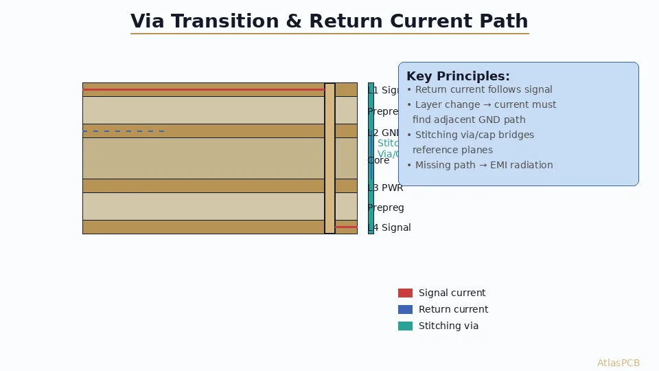
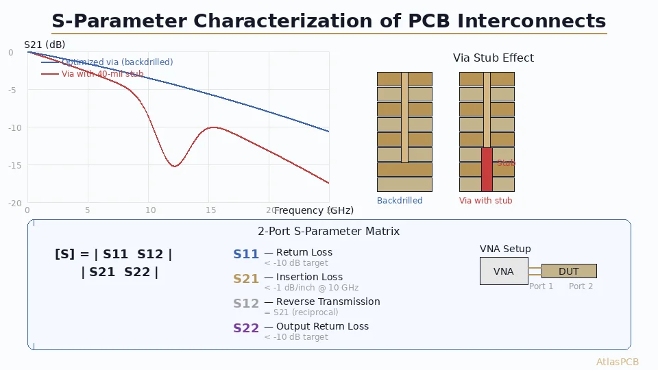
A through-hole via in a multilayer PCB behaves as a series inductance (via barrel) with shunt capacitance (pad-to-plane coupling) and a stub resonator (unused barrel below the signal layer):
Port 1 ──┤├── L_via ──┤├── Port 2
              |               |
           C_pad           C_pad
              |               |
            GND             GND
              |
          L_stub ── C_stub
              |
            GND (anti-pad)
The stub creates a quarter-wave resonance at: f_resonance = c / (4 × stub_length × √εr)
Example: 40-mil (1.0mm) stub in FR-4 (εr ≈ 4.0): f_res = 3×10⁸ / (4 × 0.001 × 2.0) = 37.5 GHz
For a typical 62-mil board with signal on layer 3 and via going through all 12 layers, the stub is much longer (~1.5mm), giving resonance at ~25 GHz — right in the bandwidth of 56 Gbps PAM4 signals.
Via Design Parameters Affecting S-Parameters
| Parameter | Effect on S21 | Effect on S11 | Optimization |
|---|---|---|---|
| Stub length | Resonant null | Resonant peak | Backdrill to ≤10 mil stub |
| Anti-pad diameter | Capacitance | Matching | 30-50 mil larger than pad |
| Pad diameter | Capacitance | Matching | Minimize (20 mil for 12 mil drill) |
| Via barrel diameter | Inductance | Minor | Match to trace impedance zone |
| Ground via proximity | Return path | Reduces S11 | 4 ground vias at ≤40 mil spacing |
Via Optimization Workflow
- Start with 3D EM simulation (Ansys HFSS, CST Studio) of the via structure including all copper layers, dielectrics, and ground vias
- Identify resonance frequency from S21 plot (look for sharp nulls)
- Adjust anti-pad to tune capacitance: larger anti-pad reduces capacitance but increases inductance
- Add ground vias to reduce return path inductance and improve S11
- Backdrill to remove stub resonance if necessary
- Validate S21 > -1 dB and S11 < -15 dB at Nyquist frequency
S-Parameters of PCB Connectors
Connector Characterization Challenges
High-speed connectors (QSFP, SFP, backplane press-fit) are the most significant S-parameter discontinuities in a PCB channel. A typical backplane connector contributes:
- 1-3 dB insertion loss at 12.5 GHz
- -8 to -12 dB return loss at Nyquist (marginal)
- 0.5-2 ns group delay
- Near-end and far-end crosstalk to adjacent pairs
Connector S-Parameter Sources
Vendor-provided .s4p files — Most connector manufacturers provide 4-port (differential) S-parameter models. Always verify against your specific PCB footprint and via structure.
Full-wave simulation — Model the connector-to-PCB transition including the via pattern, anti-pad geometry, and stripline routing. This captures the combined connector + footprint behavior.
VNA measurement — Measure production samples using a calibrated test fixture. Requires careful de-embedding of launch structures (see measurement section below).
Connector Footprint Optimization
The connector’s PCB footprint often dominates its S-parameter performance. Key optimizations:
- Via-in-pad for signal pins (eliminate dog-bone routing)
- Optimal anti-pad on each reference plane
- Ground via shield between differential pairs (reduces crosstalk)
- Controlled breakout routing with length-matched differential pairs
- Back-drilled signal vias if connector uses through-hole pins

25+ Gbps PCB Channel Design?
AtlasPCB manufactures impedance-controlled boards with ±5% tolerance, precision backdrilling, and via-in-pad for optimal S-parameter performance.
Get High-Speed PCB Quote →Transmission Line S-Parameters
Conductor and Dielectric Loss
PCB trace insertion loss has two components:
Conductor loss (αc): Increases with √f due to skin effect
αc ≈ (Rs / (Z0 × w)) × (1 / (1 + (w/h)×2/π × ln(2πw/t)))Dielectric loss (αd): Increases linearly with frequency
αd = π × f × √εr × tan(δ) / cAt low frequencies (<1 GHz), conductor loss dominates. Above 5 GHz, dielectric loss takes over — this is why material selection (Df = loss tangent) matters enormously for high-speed channels.
Material Impact on S21
| Material | Dk | Df @ 10 GHz | Loss (dB/inch @ 12.5 GHz) |
|---|---|---|---|
| Standard FR-4 | 4.2 | 0.020 | -1.8 |
| Mid-loss (Megtron 4) | 3.8 | 0.008 | -0.9 |
| Low-loss (Megtron 6) | 3.6 | 0.004 | -0.6 |
| Ultra-low-loss (Megtron 7) | 3.4 | 0.002 | -0.4 |
Design implication: A 10-inch channel on standard FR-4 loses 18 dB at 12.5 GHz — exceeding most SerDes equalization budgets. Low-loss material is mandatory for channels > 6 inches at 25 Gbps.
Differential vs. Single-Ended S-Parameters
High-speed PCB channels use differential signaling. Differential S-parameters use mixed-mode notation:
- Sdd21 — Differential insertion loss (primary design metric)
- Sdd11 — Differential return loss
- Sdc21 — Mode conversion (differential to common-mode)
- Scc21 — Common-mode insertion loss
Mode conversion (Sdc21) should be < -20 dB. High mode conversion indicates trace length mismatch, asymmetric via structures, or non-uniform dielectric around the differential pair.
VNA Measurement Methodology
Test Coupon Design
Design S-parameter test coupons on the same panel as your production board to ensure identical stackup and process conditions:
- Thru structure: Straight transmission line connecting port 1 to port 2 (known length, e.g., 3 inches)
- Reflect structure: Open or short at the end of a transmission line
- DUT structure: The via, connector, or discontinuity you want to characterize
- 2x-Thru for de-embedding: A thru structure that is exactly 2× the launch length
IEEE 370 De-Embedding
Raw VNA measurements include the test fixture (cables, connectors, PCB launches) in addition to your DUT. IEEE 370 provides standardized methods to mathematically remove fixture effects:
2x-Thru method:
- Measure a thru structure with identical launches on both ends
- The algorithm splits the thru measurement into two halves (one per launch)
- Remove launch contribution from DUT measurement
Advantage: No separate calibration kit needed. The test coupon itself provides calibration data.
Measurement Best Practices
- Calibration: Perform SOLT or ECal calibration at the cable connector plane before measurement
- Averaging: Use ≥16 averages for noise reduction
- IF bandwidth: Set to 100-1000 Hz for clean S21 measurements
- Frequency points: Minimum 1601 points over your bandwidth for adequate time-domain resolution
- Port impedance: Confirm 50Ω (single-ended) or 100Ω (differential) reference impedance
From S-Parameters to Eye Diagram Prediction
Channel Simulation Workflow
S-parameter data feeds directly into SerDes channel simulation:
- Concatenate channel segments: Combine S-parameter blocks for each via, trace segment, and connector (cascade S-to-T matrix conversion)
- Apply CTLE equalization: Model the receiver’s continuous-time linear equalizer response
- Apply FFE/DFE: Model transmitter feed-forward and receiver decision-feedback equalization
- Compute eye diagram: Convert frequency-domain channel response to time-domain pulse response, then convolve with data pattern
- Check compliance: Verify eye height > minimum (e.g., 15 mV for PCIe 5.0) and eye width > minimum (e.g., 0.3 UI)
Common Channel Budget Example (25 Gbps NRZ, 10-inch trace)
| Segment | Length | S21 @ 12.5 GHz |
|---|---|---|
| TX package + via | N/A | -1.5 dB |
| TX breakout trace | 0.5 in | -0.5 dB |
| Via transition 1 | N/A | -0.4 dB |
| Stripline trace | 8 in | -6.4 dB (Megtron 6) |
| Via transition 2 | N/A | -0.4 dB |
| Connector | N/A | -2.0 dB |
| Via transition 3 | N/A | -0.4 dB |
| Trace (card 2) | 3 in | -2.4 dB |
| RX package + via | N/A | -1.5 dB |
| Total | -15.5 dB |
With 15.5 dB total loss, a SerDes with 25 dB equalization capability has 9.5 dB margin — a comfortable design.
Practical Tips for PCB S-Parameter Optimization
- Always backdrill when via stub > 10 mil at frequencies above 10 GHz
- Use 4 ground vias around every signal via for clean return path
- Match anti-pad to impedance — simulate, don’t guess
- Request test coupons on your PCB panel for post-fabrication validation
- Correlate simulation to measurement — adjust Dk/Df in your model until simulation matches measurement within 0.5 dB
Further Reading
- PCB Back Drilling for Via Stub Removal — When and how to remove via stubs for 10+ Gbps signals
- Eye Diagram Interpretation for PCB Signal Integrity — Understanding jitter, ISI, and eye mask compliance
- Differential Pair Routing Rules for High-Speed SerDes — Maintaining impedance through routing decisions
- PCB High-Speed Material Dk/Df Comparison — Choosing the right laminate for your data rate
Building a high-speed PCB channel? AtlasPCB provides impedance-controlled fabrication with ±5% tolerance, precision backdrilling (±5 mil depth control), and TDR/VNA-validated test coupons on every high-speed panel. Get a quote for your high-speed design →
About AtlasPCB — We specialize in complex PCB manufacturing for HDI, RF, and high-reliability applications. Explore our impedance-controlled PCB manufacturing . Every order includes free engineering review. Get your quote.
Reviewed by AtlasPCB Engineering Team — IPC-certified manufacturing specialists with 15+ years of production experience in HDI, RF, and high-reliability PCB fabrication. Content based on factory floor data and real customer design reviews.
- s-parameters
- signal-integrity
- via-transition
- high-speed-design
- vna-measurement
- insertion-loss
- return-loss