· AtlasPCB Engineering · Engineering · 8 min read
BGA Underfill for PCB Assembly: Capillary, Molded and Reworkable Materials Selection Guide
Complete guide to BGA underfill selection for high-reliability PCB assemblies. Compare capillary flow, molded underfill, and reworkable formulations — with process parameters, CTE matching, and reliability data for automotive and aerospace applications.
Introduction: The Reliability Crisis at Fine Pitch
Every BGA solder joint is a mechanical link between two materials with fundamentally different thermal expansion rates. The silicon die expands at 3 ppm/°C. The organic PCB substrate expands at 14–17 ppm/°C. With every thermal cycle, these joints accumulate fatigue damage.
At 1.0 mm pitch with 0.6 mm solder balls, the joints have enough compliance to survive thousands of cycles. But as pitch shrinks to 0.5 mm, 0.4 mm, and below — driven by mobile processors, FPGAs, and AI accelerators — the solder volume decreases cubically while the strain remains constant. Without intervention, fine-pitch BGA joints fail in hundreds of cycles rather than thousands.
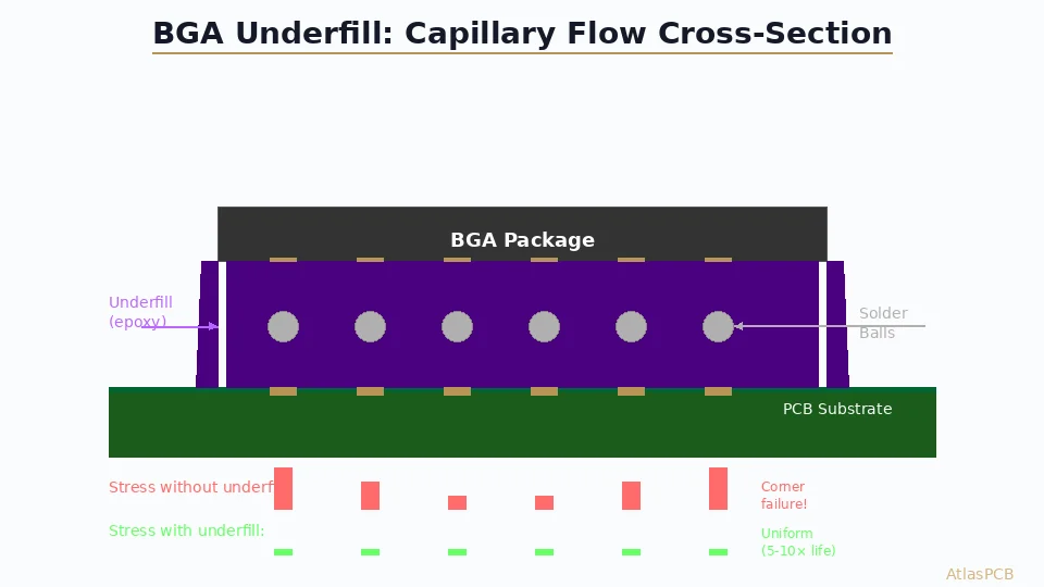
Underfill solves this problem by converting the discrete point-contact interface into a continuous area-contact bond. The epoxy matrix distributes stress uniformly, reducing peak strain at corner joints by 60–80% and extending fatigue life by 5–10×.
This guide covers the three major underfill technologies, their process requirements, and selection criteria for different reliability environments.
Underfill Mechanics: How Stress Distribution Works
Without Underfill
In an ununderfilled BGA, the stress state during thermal excursion follows the “distance from neutral point” (DNP) model:
γ = ΔT × Δα × DNP / h_standoff
Where:
- γ = shear strain on solder joint
- ΔT = temperature range
- Δα = CTE difference (package vs. PCB)
- DNP = distance from package center to joint
- h_standoff = solder ball height after reflow
Corner joints (maximum DNP) experience the highest strain and fail first. For a 35 mm BGA package with 0.4 mm pitch, corner joints see 2–3× the strain of center joints.
With Underfill
The underfill creates a composite layer that:
- Couples the package to the PCB — forces co-deformation rather than differential expansion
- Redistributes shear stress — converts concentrated solder shear to distributed interfacial shear
- Adds structural stiffness — prevents out-of-plane warpage that creates tensile stress on joints
The result: peak solder strain drops to 20–40% of the ununderfilled value, and the strain gradient across the package (corner vs. center) decreases dramatically.
Capillary Underfill: The Standard Process
Materials
Capillary underfill is a liquid epoxy formulation designed for:
- Low viscosity at dispense (5,000–30,000 cP at 25°C) for rapid flow
- High filler content (60–70% by weight silica) for CTE matching
- Fast gel time at cure temperature (3–8 minutes at 150°C)
- High Tg (>130°C) for reliable operation up to 125°C
Key Material Properties
| Property | Typical Range | Target for Fine Pitch |
|---|---|---|
| Viscosity (25°C) | 5,000–30,000 cP | < 15,000 cP |
| CTE₁ (below Tg) | 25–35 ppm/°C | 25–30 ppm/°C |
| CTE₂ (above Tg) | 80–120 ppm/°C | < 90 ppm/°C |
| Tg | 130–165°C | > 140°C |
| Modulus | 6–12 GPa | 8–10 GPa |
| Filler content | 60–70 wt% | > 65 wt% |
| Adhesion (die shear) | > 30 MPa | > 40 MPa |
Dispensing Process
Step 1: Substrate Preheat (Optional)
- Heat PCB assembly to 70–90°C on the dispense stage
- Reduces viscosity by 50–70%, accelerating flow
- Critical for large packages (> 25 mm) or gap heights < 50 μm
Step 2: Needle Dispense
- Dispense along one or two edges of the BGA package
- Needle gauge: 20–22 AWG for standard, 25 AWG for fine pitch
- Line speed: 15–30 mm/s
- Dispense weight: typically 20–50 mg per edge depending on package size
Step 3: Capillary Flow
- Underfill flows beneath the package by capillary action
- Flow time: 30–120 seconds depending on gap, viscosity, and temperature
- Flow front visible at opposite edge confirms complete fill
Step 4: Fillet Formation
- Additional dispense around remaining edges creates structural fillet
- Fillet height: 50–80% of package standoff height
Step 5: Thermal Cure
- Oven cure: 150°C for 30–60 minutes (batch)
- Snap cure: 165°C for 5–8 minutes (inline, higher throughput)
- Ramp rate: < 5°C/min to prevent void formation
Process Control Points
- Void content: Must be < 5% by area (X-ray or C-SAM inspection)
- Fillet symmetry: All four sides should show consistent fillet formation
- Flow completeness: 100% coverage required — any dry areas create stress concentrators
- Cure verification: DSC (Differential Scanning Calorimetry) confirms > 95% cure conversion
High-Reliability PCB Assembly Services
AtlasPCB offers IPC Class 3 assembly with underfill process capability for automotive, aerospace, and defense BGA packages.
Request Assembly Quote →Molded Underfill (MUF): Package-Level Solution
How MUF Works
Molded underfill combines the encapsulation and underfill steps into a single compression molding process during package assembly (not board assembly):
- Die is flip-chip bonded to substrate with flux-only (no underfill)
- Molded material is placed as pellet on the substrate
- Compression mold closes, applying heat (175°C) and pressure (5–10 MPa)
- Material flows simultaneously over the die (encapsulation) and under it (underfill)
- Cure completes in 90–120 seconds in-mold
MUF vs. Capillary: Comparison
| Aspect | Capillary Underfill | Molded Underfill |
|---|---|---|
| Process level | Board assembly | Package assembly |
| Throughput | 100–200 units/hr | 500–1000 units/hr |
| Void rate | 1–5% typical | < 0.5% (pressure) |
| Filler size limit | < 15 μm (flow) | < 30 μm (molding) |
| Gap height minimum | 30 μm | 20 μm |
| Rework capability | Difficult | Very difficult |
| Cost per unit | $0.05–0.20 | $0.01–0.05 |
When to Specify MUF
MUF is the right choice when:
- Package manufacturer controls the underfill process (standard for mobile processors)
- Ultra-fine pitch (< 0.3 mm) where capillary flow becomes unreliable
- High volume justifies compression mold tooling
- Void-free requirement is absolute (military, medical implant)
Board assemblers typically receive MUF packages already underfilled — no additional process step required during SMT assembly.
Reworkable Underfill: The Compromise
Chemistry
Standard underfill uses thermoset epoxy — once cross-linked, it cannot be softened. Reworkable formulations use:
- Thermoplastic base resins (polyamide, polysulfone blends) — soften above 200°C
- Cleavable cross-linkers — bonds break at specific temperature, allowing removal
- Reduced filler loading (45–55 wt%) — necessary for flow at lower cure temperatures
Rework Process
- Heat package locally to 220–240°C (above underfill softening point)
- Underfill softens, allowing package lift-off with vacuum nozzle
- Clean residual material from PCB pads (solvent wipe while warm)
- Inspect pads, redress if necessary
- Place new component and reflow
- Re-apply underfill and cure
Reliability Trade-off
Reworkable underfill provides approximately:
- 3–5× solder life improvement (vs. 5–10× for permanent underfill)
- Lower Tg (100–120°C vs. 140–165°C for permanent)
- Higher CTE₁ (35–45 ppm/°C vs. 25–30 ppm/°C)
- Lower adhesion strength (20–30 MPa vs. 40–50 MPa)
Use cases: Prototyping, engineering validation, repairable products (medical equipment, telecom base stations), and applications where component obsolescence may require field upgrades.
CTE Matching: The Critical Design Variable
The CTE Mismatch Problem
The package-board system has three CTE zones:
- Silicon die: 3 ppm/°C
- BGA substrate (organic): 12–16 ppm/°C
- PCB: 14–18 ppm/°C
Underfill CTE should be between the package substrate and PCB CTE values — typically 25–35 ppm/°C provides optimal stress distribution.
Filler Content and CTE
The CTE of underfill is controlled by silica filler loading:
- 0% filler: CTE ≈ 65–80 ppm/°C (pure epoxy)
- 50 wt%: CTE ≈ 40–50 ppm/°C
- 65 wt%: CTE ≈ 28–35 ppm/°C
- 75 wt%: CTE ≈ 20–25 ppm/°C (but viscosity too high for capillary)
The practical sweet spot: 65–70 wt% filler balances CTE matching against flow characteristics.
Modulus Considerations
Higher modulus underfill provides more stress redistribution but also transmits more strain to the die. The optimal modulus depends on die size:
- Small die (< 5 mm): Higher modulus OK (8–12 GPa) — die is stiff relative to package
- Large die (> 15 mm): Lower modulus preferred (5–8 GPa) — reduces die-level stress
Reliability Testing and Qualification
Standard Test Protocols
| Test | Conditions | Pass Criteria (IPC) |
|---|---|---|
| Temperature Cycling | -40°C to +125°C, 1 cycle/hr | > 1000 cycles, no crack |
| Thermal Shock | -55°C to +125°C, 10 min dwell | > 500 cycles |
| HAST | 130°C, 85% RH, 33.3 psi | > 96 hours |
| Drop Test | 1500G, 0.5 ms, 6 orientations | > 30 drops |
| Vibration | 20–2000 Hz, 20G random | > 8 hours |
Underfill Impact on Test Results
Typical improvement factors with proper capillary underfill vs. bare BGA:
| Test | Without Underfill | With Underfill | Improvement |
|---|---|---|---|
| Temp Cycling (-40/+125) | 400–800 cycles | 3000–6000 cycles | 5–8× |
| Drop (1500G) | 5–15 drops | 80–200 drops | 10–15× |
| Vibration fatigue | 2–4 hours | 20–50 hours | 8–12× |
Failure Modes with Underfill
Even with underfill, BGA assemblies eventually fail. Common failure modes shift from:
- Without underfill: Solder fatigue crack (bulk solder)
- With underfill: Interface delamination (underfill-to-passivation or underfill-to-solder-mask), or PCB pad cratering (laminate shear beneath pad)
Understanding the shifted failure mode is critical for root cause analysis.
Process Troubleshooting
Void Formation
Causes:
- Outgassing from flux residue trapped beneath BGA
- Dispense at temperature too high (premature gel before flow completes)
- Moisture in substrate or underfill material
- Excessive preheat causing material skin formation
Solutions:
- Ensure flux residue is < 3.9 μg/cm² NaCl equivalent (post-reflow clean)
- Reduce preheat temperature by 10–15°C
- Bake PCB assemblies at 125°C for 4 hours before underfill
- Use vacuum-assisted underfill dispensing for critical applications
Incomplete Flow
Causes:
- Solder mask thickness variation creating uneven gap
- Component tilt > 50 μm from coplanarity issues
- Underfill viscosity too high (expired material, storage error)
- Insufficient preheat for large packages
Solutions:
- Specify solder mask thickness tolerance ≤ ±10 μm in underfill regions
- Verify component coplanarity meets IPC-7095 requirements
- Monitor underfill viscosity batch-to-batch (reject if > 150% of spec)
- Increase preheat to 85–95°C for packages > 30 mm
Delamination After Cure
Causes:
- Cure too fast (temperature overshoot creating internal stress)
- Poor adhesion to solder mask (surface energy mismatch)
- Contamination on package passivation surface
- CTE mismatch creating interfacial stress during cool-down
Solutions:
- Use ramped cure profile (< 3°C/min to peak, then hold)
- Plasma clean PCB surface before underfill (improves adhesion 2–3×)
- Verify underfill-to-solder-mask adhesion with peel test coupons
- Select underfill with CTE₁ matched to ±5 ppm/°C of solder mask CTE
Selection Decision Framework
Application-Based Selection
Consumer Electronics (Phone, Laptop):
- MUF applied at package level (specified by component manufacturer)
- Board assembler: no underfill step required
- If board-level underfill needed: reworkable formulation
Automotive Electronics (ECU, ADAS):
- Capillary underfill, non-reworkable
- CTE₁ < 30 ppm/°C, Tg > 150°C
- Qualification: AEC-Q104 equivalent with 2000+ cycles at -40/+150°C
Aerospace/Defense:
- Capillary underfill, non-reworkable, MIL-spec qualified
- 100% X-ray inspection for voids
- Redundant fillet inspection
- Qualification: MIL-STD-883 and specific program requirements
Medical Implant:
- MUF (zero void requirement)
- USP Class VI biocompatibility certification
- Hermeticity considerations if in sealed package
Further Reading
- BGA X-Ray Void Analysis and IPC-7095 Inspection
- BGA Pad Design and Via-in-Pad Solder Voiding Prevention
- Reflow Soldering Profile Optimization for Lead-Free Assembly
- PCB CTE Mismatch and Thermal Stress in Multilayer Boards
Need PCB assemblies with BGA underfill for automotive or aerospace qualification? AtlasPCB provides IPC Class 3 assembly with controlled underfill dispensing, X-ray void inspection, and complete process documentation. Contact our engineering team for your reliability requirements.
About AtlasPCB — We specialize in complex PCB manufacturing for HDI, RF, and high-reliability applications. Explore our HDI PCB manufacturing capabilities, RF and high-frequency PCB services, or get an PCB assembly services . Every order includes free engineering review. Get your quote.
Reviewed by AtlasPCB Engineering Team — IPC-certified manufacturing specialists with 15+ years of production experience in HDI, RF, and high-reliability PCB fabrication. Content based on factory floor data and real customer design reviews.
- BGA underfill
- capillary underfill
- molded underfill
- PCB assembly
- reliability
- thermal cycling
- CTE mismatch