· AtlasPCB Engineering · Engineering · 12 min read
Reflow Soldering Profile Optimization: Lead-Free PCB Assembly Temperature Profiles for SAC305 and Beyond
Master reflow soldering profile optimization for lead-free PCB assembly. Learn thermal profiling zones, SAC305 peak temperature windows, ramp rates, and troubleshooting techniques for zero-defect BGA, QFN, and fine-pitch component soldering.

Introduction: Why Reflow Profiling Is the Most Critical PCBA Process Step
In surface mount PCB assembly, the reflow soldering process determines whether your board works or fails. Every solder joint on a modern PCB—from 0201 passive components to 1500-ball BGAs—forms simultaneously during a precisely controlled thermal cycle lasting 4-7 minutes. Get the profile wrong, and you face head-in-pillow defects on BGAs, tombstoning on chip components, cold joints on QFN ground pads, or thermal damage to sensitive ICs.
The transition from tin-lead (SnPb) to lead-free soldering raised the stakes dramatically. SAC305 alloy melts at 217-220°C versus 183°C for eutectic SnPb—a 34°C increase that pushed peak reflow temperatures dangerously close to component and PCB material thermal limits. This narrower process window demands precision profiling that accounts for board thermal mass, component density variation, and oven zone capabilities.
This guide covers everything you need to know about reflow soldering profile optimization for lead-free assembly: the physics behind each thermal zone, how to develop profiles for complex boards, troubleshooting defects through profile adjustment, and production monitoring strategies that maintain zero-defect soldering across millions of joints.
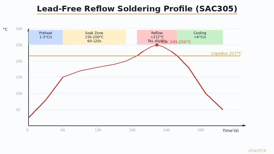
The Four Zones of a Reflow Soldering Profile
Every reflow profile, regardless of solder alloy or oven type, consists of four distinct thermal zones. Understanding the metallurgical and chemical purpose of each zone is essential for effective profiling.
Zone 1: Preheat Ramp (Ambient to 150°C)
The preheat zone raises the PCB assembly from room temperature to the beginning of thermal soak. This zone’s primary constraints are:
Ramp rate: 1.5-3.0°C/second for lead-free profiles. Faster rates cause:
- Thermal shock to ceramic components (MLCC cracking)
- Uneven board heating (warpage)
- Solder paste spattering from rapid solvent boiling
- Flux activation before oxide removal can occur
Slower ramp rates (<1.0°C/s) waste oven capacity and may cause oxidation of exposed copper and component leads before flux activates.
Target endpoint: 150°C across all board locations. At this temperature, solder paste flux begins activating and volatile solvents are mostly evaporated.
Zone 2: Thermal Soak (150-200°C, 60-120 seconds)
The soak zone is where flux chemistry does its critical work:
- Flux activation: Rosin or organic acid flux components become chemically active, dissolving metal oxides on pads, component leads, and solder powder surfaces
- Solvent evaporation: Remaining volatile vehicles escape gradually rather than explosively
- Temperature equalization: Heat conducts through the board and into large thermal-mass components (transformers, heat sinks, thick copper planes)
Profile shape options:
- Ramp-soak-spike (RSS): Traditional profile with flat soak plateau. Better for boards with high thermal mass variation.
- Ramp-to-peak (RTP): Continuous ramp without plateau. Better for uniform-density boards; reduces total time above temperature.
Most lead-free profiles use a modified RSS approach with a slight upward slope (0.5-1.0°C/s) through the soak zone rather than a true plateau.
Zone 3: Reflow (Above Liquidus 217°C)
This is where solder joints actually form. Critical parameters:
Time above liquidus (TAL): 40-90 seconds for SAC305
- Minimum 40s ensures complete wetting of all joint surfaces
- Maximum 90s prevents excessive intermetallic compound (IMC) growth and copper dissolution
- Optimal range: 50-70 seconds for most assemblies
Peak temperature: 240-250°C
- Must exceed liquidus by ≥23°C for reliable wetting
- Large-pad components (QFN exposed pads, BGA) may need higher peaks
- Never exceed component-specific maximum (check datasheets)
Delta-T (ΔT): <10°C across the board at peak
- Measured between hottest and coldest thermocouple locations
- Larger ΔT means some joints are under-reflowed while others are over-cooked
- Achieving low ΔT on large, dense boards requires careful zone optimization
Zone 4: Cooling (Peak to Solidification and Below)
Cooling rate: 2-4°C/s from peak to 150°C
The cooling zone is often neglected but critically affects solder joint reliability:
Metallurgical effects of cooling rate:
| Cooling Rate | Grain Structure | Fatigue Life | Risk |
|---|---|---|---|
| <2°C/s | Coarse grains, large Ag₃Sn plates | Reduced 30-40% | Poor long-term reliability |
| 2-4°C/s | Fine equiaxed grains | Optimal | Best balance |
| 4-6°C/s | Very fine grains | Good initially | Component stress risk |
| >6°C/s | Ultra-fine | Unknown | Ceramic cracking, delamination |
The cooling profile directly controls solder microstructure. SAC305 solidifies through a complex eutectic reaction, and the rate at which this occurs determines the distribution and size of Ag₃Sn and Cu₆Sn₅ intermetallic particles within the tin matrix.
Board-Level Thermal Challenges
Real PCBs are not uniform thermal loads. Understanding where thermal challenges arise helps you anticipate profiling difficulties.
Thermal Mass Variation
A typical mixed-technology board contains:
- High thermal mass: Large BGAs (40×40mm), shielding cans, connectors with metal housings, heat sinks, transformers
- Low thermal mass: 0201/0402 chip components, thin SOT-23 packages, discrete diodes
- Board copper distribution: Heavy ground planes act as heat sinks; signal-layer-only areas heat faster
The temperature difference between a 0402 capacitor on a signal layer and a 1156-ball BGA on a ground plane can exceed 30°C during ramp—but you need both to reach peak within 10°C of each other.
Edge vs. Center Temperature
Board edges heat faster than centers in convection ovens due to:
- Direct exposure to heating elements on edges
- Center areas shielded by surrounding board mass
- Airflow patterns in convection ovens creating temperature gradients
Mitigation strategies:
- Panel orientation: place thermally challenging areas in the center
- Conveyor speed adjustment to allow longer equalization
- Zone temperature profiling to compensate for edge/center differential
Component Shadowing
In double-sided assemblies, tall components on the topside create “shadows” in convection airflow, reducing heat transfer to surrounding areas. Similarly, large ground-plane areas on inner layers conduct heat away from surface pads, creating cold spots.
Developing a Reflow Profile: Step-by-Step Process
Step 1: Board Characterization
Before touching the oven, analyze your PCB assembly for thermal profiling challenges:
- Identify thermal extremes: Locate the highest and lowest thermal mass components
- Map copper distribution: Heavy copper areas will lag in temperature
- Note temperature-sensitive components: Check every component for max reflow temperature
- Calculate board thermal budget: Total board mass × specific heat = energy required
Step 2: Thermocouple Placement
Place thermocouples at these critical locations (minimum 5, preferably 7-9):
- Hottest expected location: Small component near board edge, away from ground planes
- Coldest expected location: Large BGA center, near heavy copper planes
- Critical component: Most expensive or failure-prone part
- Board center: Represents average temperature
- Board edge: Detects edge/center differential
- Under large QFN/BGA: Pad temperature (actual solder joint)
- Near temperature-sensitive component: Verifies safe maximum
Thermocouple attachment methods:
- High-temperature solder (Bi-Sn at 138°C won’t remelt during lead-free reflow—use high-temp Pb-free or kapton tape)
- Kapton tape for surface measurements
- Thermal paste in through-holes for internal measurement
Step 3: Initial Profile Development
Start with oven manufacturer recommendations for your board type, then iterate:
- Set zone temperatures based on target profile shape
- Run profiling board through oven at estimated conveyor speed
- Analyze thermocouple data against target windows
- Adjust zone temperatures and speed incrementally (±5°C, ±5 cm/min)
- Re-run until all thermocouples fall within specification
Typical starting points for SAC305 on 8-layer FR-4:
- Zone 1-2 (preheat): 160-180°C
- Zone 3-4 (soak): 180-200°C
- Zone 5-6 (reflow): 240-260°C
- Zone 7-8 (cooling): Fans at 80-100%
- Conveyor speed: 70-90 cm/min (depends on oven length)
Step 4: Profile Validation
A validated profile must satisfy ALL of the following simultaneously:
- Ramp rate: 1.5-3.0°C/s (all locations)
- Soak time: 60-120 seconds between 150-200°C
- Time above liquidus: 40-90 seconds (all locations)
- Peak temperature: 240-250°C (within component limits)
- ΔT at peak: <10°C
- Cooling rate: 2-4°C/s
- Total profile time: <7 minutes (to prevent excessive board exposure)
Defect Troubleshooting Through Profile Adjustment
Many assembly defects trace directly to profile parameters. Understanding these relationships enables systematic troubleshooting:
Head-in-Pillow (HiP) Defects on BGAs
Symptom: BGA ball contacts pad but doesn’t fully coalesce—looks like a head resting on a pillow. See also our guide on [BGA rework and reballing]/blog/bga-rework-reballing-process-guide/) for related techniques.
Root cause: The BGA ball and paste deposit melt at different times. If the board warps during reflow, the ball separates from the pad while molten. When they cool and come back together, oxide skins prevent coalescence.
Profile adjustments:
- Reduce time above liquidus (aim for 50-60s rather than 80-90s)
- Lower peak temperature to minimize warpage
- Increase soak time to improve temperature uniformity
- Ensure nitrogen atmosphere (<1000 ppm O₂) to reduce oxidation
Tombstoning (Component Standing on End)
Symptom: Small chip components (0402, 0603) lift off one pad and stand vertically.
Root cause: Unequal wetting force on the two pads—one end melts and wets before the other, pulling the component upright.
Profile adjustments:
- Extend soak time to improve pad temperature equalization
- Reduce ramp rate to minimize thermal gradients across small components
- Check pad design (thermal relief on pads connected to planes)
- Verify solder paste deposit equality (SPI data) — learn more about [AOI and SPI inspection]/blog/aoi-spi-inspection-pcb-assembly-quality-control/)
Voiding in QFN/BGA Thermal Pads
Symptom: X-ray shows large voids (>25% area) in thermal pad solder joints.
Root cause: Flux volatiles trapped under large, flat pads with no escape path during reflow.
Profile adjustments:
- Extend soak zone to 100-120 seconds (more time for outgassing)
- Increase soak temperature to 190-200°C (more aggressive volatile removal)
- Reduce ramp rate through soak zone
- Consider vacuum reflow for critical applications (reduces voiding to <5%)
Graping / Non-Coalescence
Symptom: Solder paste powder particles partially melt but don’t fully coalesce into a smooth joint—appears grape-like under magnification.
Root cause: Flux exhaustion before reflow peak. Common when soak zone is too long or too hot.
Profile adjustments:
- Reduce soak time (target 60-80s)
- Lower soak temperature (150-180°C)
- Switch to RTP profile shape if possible
- Evaluate paste flux activity (may need more active flux system)
Cold Joints on Large Components
Symptom: Dull, rough-surfaced joints that lack proper wetting. Common on large transformer pins or connector leads.
Root cause: Insufficient temperature or time above liquidus at the specific joint location.
Profile adjustments:
- Increase peak temperature (ensure component can tolerate it)
- Extend TAL to 70-80 seconds
- Add thermocouple directly at the cold joint location
- Consider pre-heating components or selective soldering for extreme cases
Lead-Free Alloy Variations and Their Profile Requirements
While SAC305 dominates the market, several alternative alloys require different profiling approaches:
SAC105 (Sn98.5/Ag1.0/Cu0.5)
- Liquidus: 227°C (higher than SAC305’s 217°C)
- Peak: 245-260°C
- Advantage: Lower silver content reduces cost and eliminates Ag₃Sn plates
- Challenge: Poorer wetting, requires higher peak temperatures
- Application: Consumer electronics with cost sensitivity
SN100C (Sn/Cu/Ni/Ge)
- Liquidus: 227°C
- Peak: 250-260°C
- Advantage: Low cost, good thermal fatigue resistance
- Challenge: Higher liquidus requires extended TAL, higher peak
- Application: Wave/selective soldering primarily, but used in reflow for cost-driven products
Low-Temperature Solder (Sn42/Bi58, SAC-Bi)
- Liquidus: 138°C (bismuth-tin) or 190-200°C (SAC+Bi variants)
- Peak: 170-180°C (Bi-Sn) or 220-230°C (SAC+Bi)
- Advantage: Reduced thermal stress on components and PCB
- Challenge: Lower fatigue resistance, bismuth embrittlement concerns
- Application: Temperature-sensitive products, mixed lead-free/SnPb assemblies
Need Expert Assembly Support for Your Complex PCBs?
AtlasPCB provides complete turnkey PCBA services with optimized reflow profiles for high-reliability applications. Our engineers develop custom thermal profiles for every board design.
Get Your Assembly Quote →Production Profile Monitoring and SPC
Developing a good profile is only the beginning. Maintaining consistent soldering quality across production volumes requires statistical process control (SPC) on thermal profile data.
Key Metrics to Monitor
For each production run, record and trend:
- Peak temperature (all thermocouple locations)
- Time above liquidus (each location)
- Ramp rates (preheat and cooling)
- ΔT at peak (max minus min temperature)
- Soak time and temperature range
Control Limits
Establish control limits based on your validated profile:
| Parameter | Target | UCL | LCL | Action |
|---|---|---|---|---|
| Peak temp (coldest) | 243°C | 250°C | 238°C | Stop line if exceeded |
| Peak temp (hottest) | 248°C | 255°C | 243°C | Stop line if exceeded |
| TAL (minimum) | 55s | 85s | 42s | Investigate if trending |
| ΔT at peak | 7°C | 10°C | - | Investigate above 10°C |
| Cooling rate | 3.0°C/s | 4.5°C/s | 1.5°C/s | Adjust fans |
Continuous Monitoring Systems
Modern reflow ovens incorporate inline profiling systems:
- KIC (Navigator, SPS): Real-time profile prediction from oven sensor data
- Solderstar: Profiling hardware integrated into oven conveyor
- ECD Super M.O.L.E.: Wireless in-oven profiler with multiple thermocouples
These systems alert operators to profile drift before defective product is produced, enabling preventive adjustment rather than reactive sorting.
Nitrogen vs. Air Atmosphere
The reflow atmosphere significantly affects solder joint quality, especially for lead-free alloys:
Nitrogen Benefits
- Reduced oxidation: Prevents oxide formation on molten solder surfaces
- Improved wetting: SAC305 wetting force increases 20-30% in N₂
- Lower defect rates: Eliminates head-in-pillow and non-wetting defects
- Wider process window: Allows lower flux activity pastes
- BGA yield improvement: Critical for fine-pitch (0.4mm) BGAs
Nitrogen Cost-Benefit Analysis
| Factor | Air Reflow | Nitrogen Reflow |
|---|---|---|
| O₂ level | 20.9% | 100-1000 ppm |
| N₂ consumption | - | 15-40 m³/hour |
| Annual N₂ cost | $0 | $15,000-50,000 |
| Defect rate (typical) | 50-200 DPM | 5-20 DPM |
| Rework cost savings | - | $30,000-100,000/year |
For high-reliability products (aerospace, medical, automotive) and fine-pitch assemblies, nitrogen is mandatory. For consumer products with generous pad geometries, air reflow with active flux can be acceptable.
Advanced Profile Techniques
Vapor Phase Reflow
Vapor phase (condensation) soldering uses a heated fluorinated fluid that condenses on the PCB surface, transferring heat with perfect uniformity:
- Maximum temperature: Precisely limited by fluid boiling point (230°C or 240°C fluids available)
- Advantage: Zero ΔT by physics—every surface reaches the same temperature
- Disadvantage: Slower throughput, limited peak temperature control, higher cost
- Application: Prototypes, high-reliability aerospace, complex boards with extreme thermal mass variation
Vacuum Reflow
Adding a vacuum phase during peak reflow extracts trapped gas from solder joints:
- Void reduction: Achieves <5% voiding on QFN thermal pads (vs. 15-30% in standard reflow)
- Process: Board reaches peak temperature → chamber evacuates to 5-50 mbar → holds 10-30 seconds → repressurizes → continues cooling
- Application: Power electronics, LED thermal management, automotive ECUs where thermal performance is critical
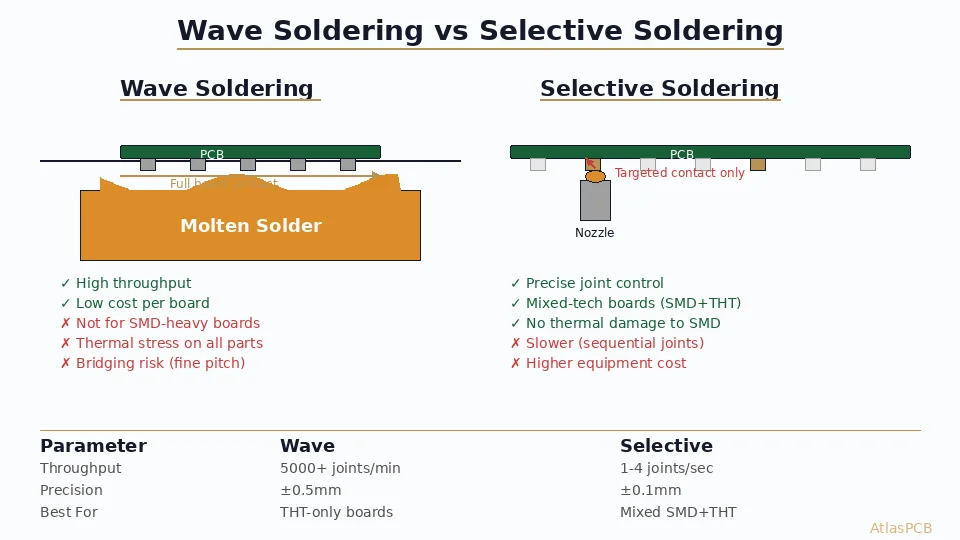
Pin-in-Paste (Intrusive Reflow)
Through-hole components reflowed with surface mount paste:
- Paste volume: 2-3× more paste deposited in/around through-holes using step stencils or print-and-dispense
- Profile consideration: THT component thermal mass often exceeds SMT; requires extended TAL
- Fill criteria: IPC-A-610 requires ≥75% vertical fill for Class 2, ≥75% + visible fillet for Class 3
- Application: Mixed-technology boards where wave soldering is undesirable
Profile Impact on Long-Term Reliability
The reflow profile doesn’t just determine initial solder joint quality—it establishes the metallurgical foundation for decades of service life.
Intermetallic Compound (IMC) Growth
Higher peak temperatures and longer TAL produce thicker initial IMC layers:
- Cu₆Sn₅: Forms at PCB pad/solder interface. Initial thickness 1-2μm, grows during service
- Ni₃Sn₄: Forms on ENIG finish. More brittle than Cu₆Sn₅ but grows slower
- Ag₃Sn: Forms within solder bulk. Plate morphology depends on cooling rate
Rule of thumb: Each additional 10°C in peak temperature adds approximately 0.3μm to initial IMC thickness, reducing long-term fatigue resistance by ~5%.
Tin Pest Risk
SAC305 is theoretically susceptible to tin pest (allotropic transformation below 13°C), though additives and impurities largely suppress it. Extended time at lower temperatures during cooling increases risk. Maintain cooling rate above 1°C/s through the 100-50°C range.
Pad Cratering
Excessive peak temperatures combined with thermal shock during cooling can initiate pad cratering—fracture within the PCB laminate beneath the pad. This latent defect may not manifest until thermal cycling in service.
Prevention:
- Peak temperature ≤250°C for FR-4 boards
- Cooling rate ≤4°C/s
- Use high-Tg laminates (Tg>170°C) for lead-free assembly (see our [PCB materials guide]/blog/high-tg-pcb-material-selection/))
- CAF-resistant materials for fine-pitch designs
Conclusion: The Profile Is Your Quality Foundation
Reflow profile optimization is not a one-time setup task—it’s an ongoing engineering discipline that directly determines your product’s solder joint quality, reliability, and field failure rate. Every new board design, paste change, or oven maintenance event warrants profile verification.
The investment in proper thermal profiling—quality thermocouples, dedicated profiling boards, SPC monitoring systems—pays returns through reduced rework, lower field failures, and faster time-to-market for new products.
Key takeaways:
- Maintain ΔT below 10°C at peak for consistent quality
- SAC305 needs 50-70 seconds above 217°C at 240-250°C peak
- Cooling rate of 2-4°C/s optimizes solder microstructure
- Monitor profiles with SPC—drift causes defects before you see them
- Use nitrogen for fine-pitch and high-reliability applications
Need help optimizing assembly processes for your next PCB project? AtlasPCB’s engineering team provides complete DFM review and turnkey assembly with custom reflow profiles for every design. Request a quote to discuss your assembly requirements.
Further Reading
- [PCB Design for GaN and SiC Power Devices: Thermal Management, Layout Rules, and Material Selection]/blog/pcb-design-gan-sic-power-devices-thermal-layout/)
- [AI Hardware PCB Thermal Management: Advanced Multilayer Stackup Design for 1000W+ Processing Units]/blog/ai-hardware-pcb-thermal-management-multilayer-design/)
- [Aluminum PCB Thermal Design for High-Power LED and Motor Drivers: Material Selection, Stackup, and DFM Guide]/blog/aluminum-pcb-thermal-design-led-motor-driver/)
- [PCB Thermal Management: Heat Dissipation Techniques for Reliable Electronics]/blog/pcb-thermal-management/)
- [Aluminum PCB for LED Applications: Design, Benefits, and Best Practices]/blog/aluminum-pcb-led-applications/)
- Rigid PCB Manufacturing
About AtlasPCB — We specialize in complex PCB manufacturing for HDI, RF, and high-reliability applications. Explore our HDI PCB manufacturing capabilities, PCB assembly services, or get an aluminum and metal-core PCB services . Every order includes free engineering review. Get your quote.
Reviewed by AtlasPCB Engineering Team — IPC-certified manufacturing specialists with 15+ years of production experience in HDI, RF, and high-reliability PCB fabrication. Content based on factory floor data and real customer design reviews.
- reflow soldering
- lead-free
- SAC305
- thermal profile
- PCB assembly
- BGA soldering
- PCBA
- DFM