· AtlasPCB Engineering · Engineering · 10 min read
BGA X-Ray Void Analysis: Inspection Methods, IPC-7095 Criteria, and Defect Classification for High-Reliability Assembly
Learn how to perform BGA X-ray void analysis using 2D transmission and 3D CT inspection. Understand IPC-7095 acceptance criteria, void percentage calculation methods, defect classification, and practical thresholds for Class 2 and Class 3 assemblies.
Introduction: Why X-Ray Void Analysis Matters for BGA Assembly
Ball Grid Array (BGA) components present a unique quality control challenge: their solder joints are hidden beneath the package body, invisible to optical inspection. Unlike QFP or chip component joints where a visual check reveals wetting quality, BGA interconnects require X-ray inspection to assess joint integrity, detect voids, identify bridging, and verify head-in-pillow defects.
Void analysis is the most critical X-ray measurement for BGA reliability. Gas pockets trapped within solder joints during reflow reduce thermal conductivity proportionally to void area, increase electrical resistance in power connections, and create mechanical stress concentrators that accelerate fatigue crack propagation under thermal cycling. For a typical BGA in a server environment experiencing 1,000+ power cycles per year, a 30% void can reduce joint fatigue life by 40–60% compared to a void-free joint.
This guide covers the physics of X-ray void detection, practical inspection workflows, IPC-7095D acceptance criteria, and the critical differences between 2D radiography and 3D computed tomography (CT) scanning that every process engineer must understand.
The Physics of X-Ray Inspection for Solder Joints
How X-Rays Reveal Voids
X-ray imaging works on the principle of differential absorption. When X-ray photons pass through a BGA assembly, dense materials (solder alloys containing tin, silver, and copper) absorb significantly more radiation than lighter materials (PCB substrate, silicon die, and gas-filled voids).
The resulting image shows solder-filled regions as bright areas (high absorption) and voids as dark spots (low absorption, X-rays pass through easily). The contrast ratio between solder and void is approximately 8:1 at typical inspection energies (80–130 kV), providing excellent detectability for voids as small as 25 μm in diameter.
Key parameters affecting void detection:
- Tube voltage (kV): Higher voltage penetrates thicker assemblies but reduces contrast. Typical BGA inspection: 80–110 kV
- Geometric magnification: Ratio of source-to-detector distance vs. source-to-sample distance. Higher magnification = better resolution but smaller field of view
- Focal spot size: Determines ultimate resolution. Micro-focus tubes (5–10 μm spot) achieve 2–5 μm feature resolution
- Integration time: Longer exposure reduces noise but extends cycle time. Balance at 0.5–4 seconds per frame
2D Transmission Radiography
In 2D X-ray inspection, the X-ray source illuminates the sample from one angle (typically perpendicular to the board surface), and a flat-panel detector captures the transmission image. All features through the full board thickness are projected onto a single 2D plane.
Advantages:
- Fast: 30–60 seconds per BGA for automated void analysis
- High throughput: Compatible with production-speed inspection
- Good for initial screening and SPC monitoring
- Lower equipment cost ($200K–$500K vs. $800K–$2M for CT)
Limitations:
- Overlapping features from top-side and bottom-side components
- Voids at different Z-positions appear in the same image, inflating apparent void area
- Cannot distinguish between a single large void and multiple small voids stacked vertically
- Oblique angle views (15–70°) partially mitigate overlap but introduce geometric distortion
3D Computed Tomography (CT)
CT scanning rotates the X-ray source (or sample) through 360°, capturing 400–1600 projection images. Reconstruction algorithms (filtered back-projection or iterative) compute the 3D density distribution, allowing engineers to:
- Slice through the solder joint at any Z-plane
- Measure individual void volumes with ±2% accuracy
- Identify void location (pad interface vs. mid-joint vs. ball center)
- Detect process-specific defect signatures
Resolution classes:
- Standard CT (10–30 μm voxel): Good for void counting in large BGAs (≥ 0.8 mm pitch)
- Micro-CT (1–5 μm voxel): Required for fine-pitch BGAs (≤ 0.4 mm) and failure analysis
- Nano-CT (50–500 nm voxel): Research applications, intermetallic growth analysis
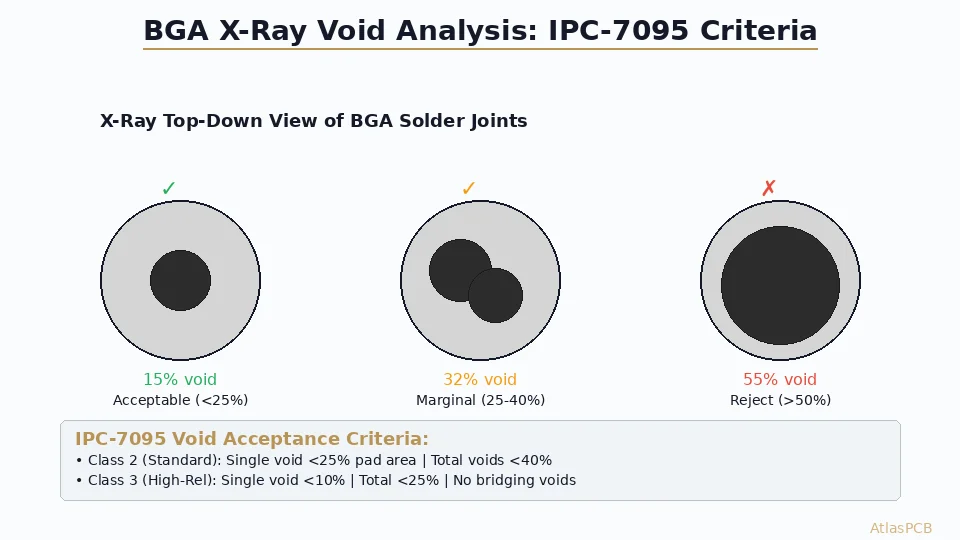
IPC-7095D Void Acceptance Criteria
Class Definitions
IPC-7095D “Design and Assembly Process Implementation for BGAs” defines void acceptance criteria aligned with IPC-A-610 product classes:
| Class | Application | Max Void Area (% of pad) |
|---|---|---|
| Class 1 | General electronics | 50% |
| Class 2 | Dedicated service | 25–30% |
| Class 3 | High performance | 25% (individual), no void > 10% pad diameter |
Measurement Methodology
The standard specifies void measurement using area ratio method:
- Define the pad boundary circle (diameter = land pad diameter)
- Identify all void regions within the boundary using grayscale thresholding
- Sum void pixel areas: A_void = Σ(void pixel count × pixel area)
- Calculate: Void% = (A_void / A_pad) × 100%
Critical notes:
- Measure at perpendicular incidence (0° tilt) for area-based criteria
- For oblique-angle systems, apply geometric correction factor
- Report the maximum void percentage across all joints, not the average
- Track SPC data per package position (corner balls, center thermal pad, etc.)
Thermal Pad Special Requirements
Large thermal/ground pads under BGA centers have different criteria because they serve as the primary heat conduction path. Excessive voiding in thermal pads directly degrades thermal resistance:
- Typical requirement: < 50% void for Class 2 thermal pads
- High-power applications: < 25% void (customer specification)
- Automotive ADAS: < 20% void with specific void location restrictions
Need High-Reliability BGA Assembly with Guaranteed Void Control?
AtlasPCB offers X-ray inspection with void analysis reporting on every BGA joint. Our Class 3 assembly process delivers < 15% void rates on fine-pitch BGAs.
Get a Quote →Practical X-Ray Inspection Workflow
Equipment Selection
Modern BGA inspection systems fall into three categories:
Inline X-ray (AXI — Automated X-ray Inspection):
- Throughput: 2–10 panels/minute depending on BGA count
- Resolution: 10–25 μm feature size
- Use case: 100% production screening, SPC monitoring
- Examples: Nordson DAGE Quadra, Nikon XT V 130C, Viscom X8011
Offline manual X-ray:
- Resolution: 0.5–5 μm with micro-focus tube
- Use case: Failure analysis, process development, first article inspection
- Full rotation capability for 3D reconstruction
- Examples: Nordson DAGE XD7800, Yxlon Cheetah EVO, Nikon XTH series
CT systems (lab-grade):
- Resolution: 1–5 μm voxel for BGA-sized samples
- Use case: Definitive void measurement, failure analysis, correlation studies
- Scan time: 5–30 minutes per component
- Examples: Zeiss Xradia, Nikon XTH 225, North Star Imaging
Image Acquisition Best Practices
Magnification: Set geometric magnification to resolve individual voids ≥ 50 μm. For 0.4 mm pitch BGA, minimum 10× magnification (effective pixel size < 15 μm)
Voltage and current: Start at 90 kV, 8W for standard 1.2 mm BGA + 1.6 mm PCB stack. Increase voltage for thicker assemblies; decrease for better void contrast
Multi-angle imaging: Capture at 0°, +30°, and –30° tilt. The oblique views separate overlapping features and reveal bridging between adjacent balls
Reference calibration: Include a known void standard (calibration phantom) in each inspection batch for threshold consistency
Automated Void Analysis Software
Modern X-ray systems include integrated void analysis:
- Board recognition: Identify BGA location from Gerber/ODB++ overlay
- Ball detection: Locate each solder ball center using circular Hough transform
- Pad boundary: Define measurement region (typically pad diameter + 5%)
- Thresholding: Adaptive grayscale threshold separating solder from void
- Void measurement: Area calculation per ball, statistics across package
- Pass/fail judgment: Compare against programmed limits per pad position
Defect Classification Beyond Voids
Head-in-Pillow (HIP) Defects
Head-in-pillow occurs when the BGA ball (head) and paste deposit (pillow) partially reflow but fail to fully coalesce. X-ray signature: a thin low-density line separating two solder hemispheres.
Root causes:
- Component warpage during reflow (> 75 μm coplanarity)
- Insufficient paste volume or height
- Ball oxidation from moisture absorption (MSL violation)
- Peak temperature too low or time above liquidus too short
X-ray identification: Look for joints with a horizontal dark line at approximately mid-height, particularly at package corners where warpage is maximum.
Solder Bridges
Bridges appear as continuous high-density paths between adjacent balls. Detectable at 0° (overhead view) when bridge is lateral, or at oblique angles when bridge forms along the row direction.
Non-Wet Open Joints
Complete wetting failure shows as separated ball and pad with no metallurgical bond. X-ray shows the ball sitting above the pad with a clear gap. Distinguished from HIP by the complete separation versus partial contact.
Insufficient Solder Volume
Balls appear smaller than nominal diameter, typically from paste printing issues or excessive via wicking. Measure ball diameter against nominal and flag if < 80% expected volume.
2D vs. CT Void Correlation: Understanding the Measurement Gap
Why 2D Overestimates Voids
A solder ball is a 3D hemisphere approximately 300–500 μm in diameter (for typical BGAs). When imaged from above, the X-ray path length through solder varies from maximum at the center to zero at the edges. A small spherical void (50 μm diameter) located at any Z-position within the ball projects its shadow onto the 2D image.
The overestimation occurs because:
- Multiple small voids at different heights project overlapping shadows
- The circular void projection appears as if all voids are in the same plane
- Background noise near the ball edge (thin solder) can be misclassified as voids
Quantified correlation:
- Boards measuring 20% void on 2D X-ray typically show 12–16% on CT
- The correction factor ranges from 0.6 to 0.8 depending on void distribution
- Establish your own correction factor by CT-scanning 20–50 representative joints
When to Use Each Method
| Scenario | Recommended Method |
|---|---|
| Production screening (100%) | 2D AXI |
| First article inspection | 2D + CT sample |
| Process qualification | CT (full statistics) |
| Customer complaint / failure | CT mandatory |
| SPC monitoring | 2D with established correlation |
| Thermal pad assessment | CT (location matters) |
Process Optimization Based on X-Ray Data
Void Reduction Strategies
When X-ray analysis reveals excessive voiding, correlate void characteristics with root causes:
Scattered small voids (< 100 μm):
- Likely cause: Flux outgassing during reflow
- Solution: Optimize reflow profile—extend preheat to evaporate volatiles; increase time above liquidus by 10–15 seconds; consider lower-voiding flux chemistry
Single large void (> 200 μm) centered under ball:
- Likely cause: Via outgassing (via-in-pad without proper fill)
- Solution: Verify via fill quality (IPC-4761 Type VII), ensure cap plating flatness ±1 mil, perform adequate bake-out (125°C, 4–8 hours) before assembly
Voids clustered at pad interface:
- Likely cause: Poor wetting from pad contamination or insufficient reflow temperature
- Solution: Check pad surface finish quality (ENIG nickel thickness 3–6 μm, immersion gold 0.05–0.1 μm); verify peak temperature ≥ SAC305 minimum (235°C recommended 240–245°C)
Asymmetric voids (one side of ball):
- Likely cause: Board warpage creating uneven contact during reflow
- Solution: Address board flatness, consider vacuum reflow for high-value assemblies
Statistical Process Control (SPC) with X-Ray Data
Implement real-time SPC using automated void measurement:
- UCL (Upper Control Limit): Set at process capability + 3σ, but never above IPC class limit
- Target: Process average should be < 50% of acceptance limit for adequate margin
- Trending: Track void% per package position over time; rising trends indicate process drift
- Cpk target: > 1.67 for high-reliability applications
Advanced Techniques: Void Analysis for Next-Generation Packages
2.5D/3D IC Packages (HBM, CoWoS)
High-bandwidth memory (HBM) stacks and chiplet architectures use micro-bumps (20–40 μm pitch) that are below the resolution of standard 2D X-ray systems. CT scanning at < 2 μm voxel size is mandatory for void assessment of:
- Micro-bump joints (C4 bumps, Cu-pillar/solder cap)
- Through-silicon via (TSV) connections
- Interposer-to-substrate ball joints
Package-on-Package (PoP)
PoP assemblies create two BGA interfaces stacked vertically. 2D X-ray imaging produces severe overlap between top and bottom package joints. Solutions:
- Oblique angle imaging: 40–60° tilt separates top and bottom layers
- Laminography: Limited-angle CT that reconstructs individual planes without full 360° rotation
- Dual-energy imaging: Two exposures at different kV settings allow material separation algorithms to distinguish layers
Internal Links and Resources
For related PCB assembly and quality topics, see:
- [BGA Pad Design and Via-in-Pad: Preventing Solder Voiding]/blog/bga-pad-design-via-in-pad-solder-voiding/) — Upstream design techniques to minimize voids before assembly
- [PCB Electrical Testing: Flying Probe vs. Fixture]/blog/pcb-electrical-testing-flying-probe-vs-fixture/) — Complementary electrical test methods for assembled boards
- [Reflow Soldering Profile Optimization for Lead-Free Assembly]/blog/reflow-soldering-profile-optimization-lead-free-pcb-assembly/) — Profile tuning to reduce void formation
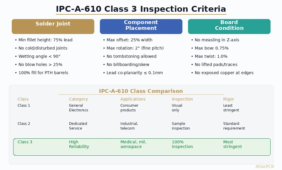
- [IPC-A-610 Class 3 Inspection Workmanship Standards]/blog/ipc-a-610-class-3-inspection-workmanship-high-reliability/) — Visual inspection criteria that complement X-ray
Conclusion
BGA X-ray void analysis is not optional for high-reliability electronics—it is the only inspection method capable of quantifying internal joint quality for hidden interconnects. Understanding the fundamental differences between 2D transmission X-ray and 3D CT scanning, applying correct IPC-7095D acceptance criteria by product class, and establishing proper measurement correlation factors between methods enables engineering teams to make confident accept/reject decisions.
For production environments, implement automated 2D X-ray with validated thresholding algorithms and SPC monitoring. Reserve CT scanning for process qualification, failure analysis, and periodic correlation verification. When void levels approach acceptance limits, use the defect classification framework to identify root causes and implement targeted process corrections.
Ready to discuss your BGA assembly requirements? Contact AtlasPCB Engineering for a consultation on our X-ray inspection capabilities and high-reliability assembly process.
Further Reading:
- [BGA Rework and Reballing Process Guide]/blog/bga-rework-reballing-process-guide/)
- [PCB Reliability Testing Methods]/blog/pcb-reliability-testing/)
About AtlasPCB — We specialize in complex PCB manufacturing for HDI, RF, and high-reliability applications. Explore our HDI PCB manufacturing capabilities, PCB assembly services, or get an full PCB manufacturing capabilities . Every order includes free engineering review. Get your quote.
Reviewed by AtlasPCB Engineering Team — IPC-certified manufacturing specialists with 15+ years of production experience in HDI, RF, and high-reliability PCB fabrication. Content based on factory floor data and real customer design reviews.
- BGA
- X-ray inspection
- void analysis
- IPC-7095
- CT scanning
- solder joint
- PCB assembly
- quality control
- AOI
- reliability testing