· AtlasPCB Engineering · Engineering · 7 min read
PCB CTE Mismatch and Thermal Stress: Prevention Strategies for Multilayer Board Reliability
Understand how coefficient of thermal expansion (CTE) mismatch causes PCB failures. Learn to calculate z-axis stress, select compatible materials, design via structures for thermal cycling survival, and validate reliability through IST and thermal shock testing.
The Physics of CTE Mismatch in PCBs
Every multilayer PCB is a composite structure — layers of copper, glass-reinforced resin, and plated through-holes bonded together into a monolithic assembly. When temperature changes, each material wants to expand at its own rate. The resulting mechanical stress is the single largest cause of PCB field failures in thermally demanding environments.
Understanding CTE (Coefficient of Thermal Expansion) mismatch is essential for any engineer designing boards for automotive, aerospace, industrial, or telecom applications where thermal cycling is unavoidable.
Material CTE Properties
In-Plane vs Z-Axis: The Critical Asymmetry
FR-4 is anisotropic — its properties differ dramatically by direction:
| Direction | CTE (ppm/°C) | Constraining Factor |
|---|---|---|
| X-axis (warp) | 12-14 | Glass weave constrains expansion |
| Y-axis (fill) | 14-16 | Glass weave constrains expansion |
| Z-axis (thickness) | 50-70 | Resin dominates, no glass constraint |
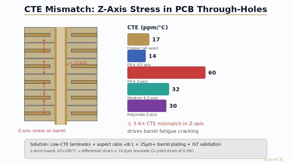
Copper, by contrast, expands uniformly at 17 ppm/°C in all directions. This creates a severe mismatch in the z-axis: the board wants to expand 3-4× faster than the copper barrel plating inside through-holes.
The Math of Stress Accumulation
For a 2.4mm thick board undergoing a 100°C temperature excursion:
Z-axis board expansion: 2.4mm × 60 ppm/°C × 100°C = 14.4 µm
Copper barrel expansion: 2.4mm × 17 ppm/°C × 100°C = 4.1 µm
Differential strain: 14.4 - 4.1 = 10.3 µm
Strain on copper: 10.3 / 2400 = 0.43%
Copper’s yield strain is approximately 0.3%. This means every single thermal cycle plastically deforms the barrel copper — a recipe for low-cycle fatigue failure.
Failure Mechanisms
Barrel Crack (Most Common)
The plated copper barrel stretches beyond yield during heating, then is compressed during cooling. After repeated cycles, fatigue cracks initiate at stress concentration points:
- Inner-layer connection interfaces (most common)
- Barrel mid-span (thinnest copper location)
- Knee of the via (where barrel meets capture pad)
A barrel crack manifests as intermittent open circuits — the crack closes under thermal expansion (hot) and opens when cool. This makes field diagnosis extremely difficult.
Corner Crack at Inner Layer Connections
Where the barrel meets an inner layer pad, a geometric stress concentration exists. The copper must transition from a cylindrical barrel to a flat pad, creating a stress riser. IPC-6012 requires minimum 25µm copper at these intersections.
Pad Lifting and Delamination
When CTE mismatch stress exceeds the adhesion strength between copper and laminate, delamination occurs. Contributing factors include:
- Moisture absorption (weakens Cu-resin bond)
- Inadequate surface roughening before lamination
- Contamination at interfaces
- Excessive thermal excursion rate
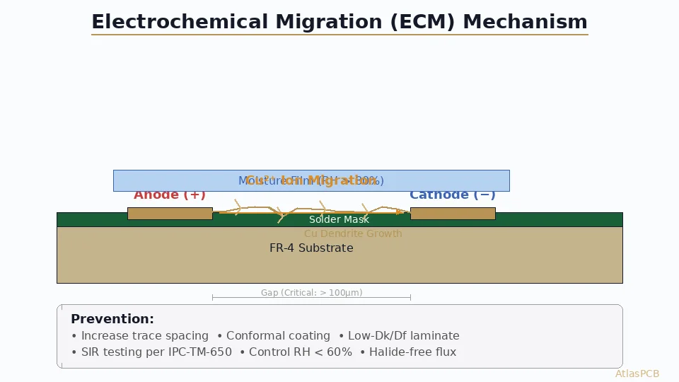
Glass-Resin Interface Failure (CAF)
Conductive Anodic Filament (CAF) growth occurs when moisture migrates along glass-resin interfaces that have been mechanically separated by CTE stress. The separated interface creates a pathway for electrochemical migration between adjacent conductors at different potentials.
High-Reliability PCBs for Demanding Environments
AtlasPCB specializes in Class 3 and automotive-grade boards with IST-validated via reliability. We select optimal materials and stackups to survive your thermal cycling requirements.
Request Reliability Consultation →Material Selection for CTE Control
Low-CTE Laminate Systems
| Material | Z-CTE (ppm/°C) | Tg (°C) | Td (°C) | Best For |
|---|---|---|---|---|
| Standard FR-4 | 55-65 | 130-140 | 310 | Consumer electronics |
| Mid-Tg FR-4 | 45-55 | 150-160 | 325 | Industrial |
| High-Tg FR-4 | 40-50 | 170-180 | 340 | Automotive |
| Megtron 6 | 30-35 | 185 | 410 | Telecom, server |
| IS680 AG | 38-42 | 200 | 360 | High-reliability |
| Polyimide | 30-35 | 250+ | 400 | Aerospace |
| BT Resin | 35-45 | 185 | 380 | IC substrates |
The Glass Transition Temperature (Tg) Connection
Below Tg, the resin is in a glassy state with relatively controlled CTE (typically 40-60 ppm/°C z-axis). Above Tg, CTE increases dramatically — often doubling to 200-300 ppm/°C. This is why lead-free soldering (peak 260°C) is so much more stressful than SnPb (peak 225°C): the resin spends more time above Tg during reflow.
Selecting high-Tg materials (>170°C) ensures the board remains in its lower-CTE state throughout normal operating conditions. For automotive under-hood applications (operating up to 150°C), a Tg of 180°C+ provides minimal margin; polyimide (Tg 250°C+) is often specified.
Decomposition Temperature (Td) Matters for Lead-Free
Td measures when the resin begins irreversible chemical degradation. During lead-free reflow at 260°C peak, the board sees temperatures between Tg and Td. Materials with Td < 320°C risk losing 2-5% mass per reflow cycle, creating internal voids that concentrate stress during subsequent thermal cycling.
Via Design for CTE Survival
Aspect Ratio Limits
Higher aspect ratios (board thickness ÷ drill diameter) mean more copper must stretch in the z-axis:
| Reliability Class | Max Aspect Ratio | Rationale |
|---|---|---|
| IPC Class 2 | 10:1 | Standard commercial |
| IPC Class 3 | 8:1 | High reliability |
| IPC ES (Automotive) | 6:1 | Maximum strain reduction |
| Aerospace/Defense | 5:1 | Conservative design |
For a 2.4mm board meeting Class 3 requirements, minimum drill diameter should be 0.3mm (12 mil). Smaller drills require either thinner boards or acceptance of higher failure risk.
Copper Plating Thickness
Thicker barrel plating distributes strain over a larger cross-section, reducing peak stress:
- Minimum 25µm: IPC Class 3 requirement
- Target 30-35µm: Recommended for automotive
- Ductility matters: High-elongation copper plating (>15% elongation) resists fatigue better than hard, brittle deposits
Specify “high-throw” plating chemistry that deposits uniform copper even at high aspect ratios. The mid-barrel location always plates thinnest — this is where failures initiate.
Via Fill and Plugging
Filled (resin-plugged or copper-filled) vias eliminate the trapped air volume that expands differently from surrounding materials. For via-in-pad designs, copper filling followed by planarization provides the most reliable result because it creates a solid copper column rather than a hollow barrel.
Design Strategies to Mitigate CTE Stress
1. Symmetric Stackup Construction
An asymmetric stackup (different materials or copper distribution above vs below midplane) warps during thermal cycling as each half expands differently. Always design symmetric stackups to minimize bow and twist.
2. Copper Balancing
Large copper-free areas on inner layers allow localized dielectric expansion that isn’t present where copper constrains the resin. Adding dummy copper fill (with thermal relief connections to ground) on all layers ensures uniform z-axis expansion across the board area.
3. Controlled Aspect Ratio
Rather than one thick board, consider:
- Two thinner boards connected by rigid-flex
- Sequential lamination to create shorter via segments
- HDI microvias (laser drilled, 5:1 aspect ratio max)
Each microvia segment is only 60-100µm deep, experiencing negligible CTE strain.
4. Annular Ring Sizing
Larger annular rings at inner-layer connections reduce stress concentration at the barrel-pad interface. IPC Class 3 requires minimum 50µm annular ring after registration tolerance. For extreme reliability, specify 100µm minimum annular ring.
5. Drill-to-Copper Clearance
Non-functional pads (inner layers where a via passes through without connection) should be removed. They constrain the barrel at points that don’t need electrical connection, adding stress concentration without benefit. IPC calls this “non-functional pad removal” — standard practice for Class 3 designs.
Testing and Validation
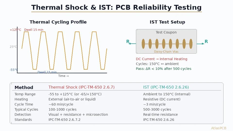
Interconnect Stress Test (IST) — IPC-TM-650 2.6.26
IST is the gold standard for via reliability assessment. A daisy-chain test coupon is repeatedly heated by internal resistance (I²R heating) from ambient to 150°C or 190°C, and resistance is continuously monitored.
- Pass criteria: <10% resistance increase after specified cycles
- Typical requirement: 500 cycles for automotive, 200 for commercial
- Acceleration factor: ~2-3× vs air-to-air thermal cycling
Thermal Shock vs Thermal Cycling
| Test | Temperature Range | Dwell Time | Transfer | Standard |
|---|---|---|---|---|
| Thermal cycling | -55 to +125°C | 10-15 min | <5 min | IPC-TM-650 2.6.7 |
| Thermal shock | -55 to +125°C | 5 min | <10 sec | MIL-STD-202 Method 107 |
| Liquid-to-liquid | -55 to +125°C | 2 min | <10 sec | IPC-TM-650 2.6.7.2 |
Thermal shock (rapid transition) is more damaging than cycling because the material has no time to relieve stress through viscoelastic creep.
Microsection Analysis
Cross-sectional analysis after testing reveals:
- Barrel copper thickness uniformity
- Crack initiation locations
- Inner-layer connection integrity
- Resin fill quality
- Delamination evidence
IPC-A-600 provides acceptance criteria for microsection evaluation across Class 1/2/3.
Case Study: Automotive ECU Failure
An automotive ECU experienced intermittent communication failures after 3 years in under-hood service. Root cause analysis revealed:
- Board: 3.2mm, 12-layer, 0.3mm via drill (aspect ratio 10.7:1)
- Material: Standard 140°C Tg FR-4
- Environment: -40 to +125°C daily cycling
- Failure mode: Barrel crack at layer 6 inner connection
Contributing factors:
- Aspect ratio exceeded Class 3 limit (8:1)
- Low-Tg material in high-temperature environment
- Copper plating only 18µm at mid-barrel
- No IST validation before production release
Corrective design:
- Changed to Megtron 6 (Tg 185°C, z-CTE 32 ppm/°C)
- Increased drill to 0.4mm (aspect ratio 8:1)
- Specified 30µm minimum barrel plating
- Added IST coupon to production panel
- Reduced board thickness to 2.8mm via HDI layer reduction
Further Reading
- HDI Via Reliability and Thermal Cycling
- PCB Warpage Control in Multilayer Boards
- High-Layer Count PCB Design Challenges
- Controlled Impedance PCB Stackup Design Rules
Designing for harsh thermal environments? AtlasPCB’s engineering team validates every high-reliability design with IST testing and recommends optimal material/stackup combinations for your operating conditions. Get a reliability assessment →
About AtlasPCB — We specialize in complex PCB manufacturing for HDI, RF, and high-reliability applications. Explore our multilayer PCB fabrication up to 30 layers, or get an aluminum and metal-core PCB services . Every order includes free engineering review. Get your quote.
Reviewed by AtlasPCB Engineering Team — IPC-certified manufacturing specialists with 15+ years of production experience in HDI, RF, and high-reliability PCB fabrication. Content based on factory floor data and real customer design reviews.
- pcb reliability
- CTE mismatch
- thermal stress
- multilayer pcb
- via reliability
- material selection