· AtlasPCB Engineering · Engineering · 8 min read
How to Specify PCB Board Thickness: Standard Options, Tolerances, and Fab Drawing Requirements
Complete guide to specifying PCB board thickness in your fabrication drawing. Covers standard thickness values, IPC tolerance classes, stackup-driven thickness control, and common mistakes that delay quotes.
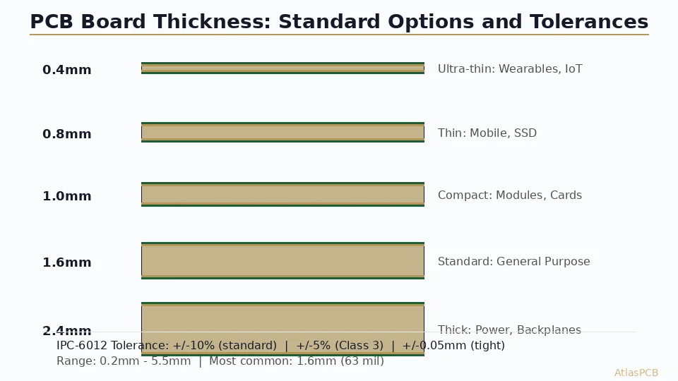
Quick Reference: Standard PCB Thicknesses
| Thickness | Layers (typical) | Common Application | Core Availability |
|---|---|---|---|
| 0.2-0.4mm | 1-2 | Flex-to-rigid transition, wearables | Limited, special order |
| 0.6mm | 2-4 | IoT modules, thin cards | Standard |
| 0.8mm | 4-6 | Mobile devices, SSD | Standard |
| 1.0mm | 4-8 | Compact modules, DIMM | Standard |
| 1.2mm | 6-8 | Networking cards, NVMe | Standard |
| 1.6mm | 4-12 | General purpose (industry default) | Standard |
| 2.0mm | 8-16 | Power electronics, backplanes | Standard |
| 2.4mm | 10-20 | Heavy copper, high-layer-count | Standard |
| 3.2-5.5mm | 16-30 | Thick backplanes, extreme multilayer | Special order |
Rule of thumb: Every additional standard FR-4 core adds 0.1-0.2mm. Every prepreg sheet adds 0.05-0.12mm depending on glass style and resin content.
Why Board Thickness Specification Matters
Getting board thickness right affects far more than mechanical fit. The dielectric thickness between copper layers directly determines impedance, and impedance determines signal quality. A 10% variation in total board thickness might seem acceptable for mechanical clearance, but if that variation concentrates in one dielectric layer (which it often does — resin flow during lamination is not perfectly uniform), your 50-ohm trace could shift to 45 or 55 ohms on that layer pair, failing TDR verification.
The second critical interaction is with via reliability. The aspect ratio — board thickness divided by drilled hole diameter — determines how well electroplating copper distributes down the via barrel. Standard mechanical drilling supports aspect ratios up to 10:1 reliably, and up to 16:1 with advanced plating processes. A 2.4mm board with 0.15mm drills hits 16:1, which sits at the limit of most fabricators’ capabilities. Specifying a thicker board without adjusting your minimum drill size is a common DFM error that causes either plating voids or forces the fabricator to increase drill sizes (breaking your routing rules).

Third, the board must physically fit its housing. This sounds obvious, but the tolerance stack between board thickness, connector seat depth, thermal interface material, and heat sink clearance catches many designers. A 1.6mm board with +/-10% tolerance means 1.44-1.76mm — a 0.32mm range that can cause interference in tight enclosures or insufficient contact pressure on thermal pads.
STACKUP ENGINEERING
Need a Custom Stackup with Tight Thickness Control?
AtlasPCB builds boards from 0.2mm to 5.5mm with +/-0.05mm tolerance when required. We provide impedance-modeled stackup proposals with exact material callouts.
Request Stackup Proposal ›How to Call Out Thickness on Your Fab Drawing
The fab drawing is where thickness specification lives, and ambiguity here delays quotes. A proper thickness callout includes four elements:
The nominal value states your target thickness — typically chosen from standard values to minimize cost. Write it clearly in the drawing notes: “Finished Board Thickness: 1.60mm.” Use millimeters consistently (not a mix of mm and mils) to avoid conversion errors.
The tolerance defines the acceptable range. Explicit is always better than relying on IPC class defaults, because not every fabricator interprets “Class 2 tolerance” identically when applied to non-standard thicknesses. Write: “Thickness Tolerance: +/-0.10mm” or ”+/-10%, whichever is less.” For card-edge connectors and press-fit applications, specify +/-0.05mm and expect a small cost premium for the tighter process control.
The measurement location clarifies where the thickness applies. On a board with large copper pours on outer layers versus isolated traces, the effective lamination pressure differs, creating thickness variation across the panel. Specify: “Thickness measured over bare laminate area (no copper).” This removes copper plating and trace height from the measurement, giving the fabricator a clear target.
The reference point indicates whether solder mask is included. Standard IPC practice excludes solder mask from the thickness measurement, but some automotive and military specs include it. If your mechanical interface cares about the actual physical envelope, state: “Finished thickness including solder mask: 1.65mm +/-0.08mm” to eliminate any ambiguity.
Thickness vs Impedance: The Critical Interaction
For any impedance-controlled design, board thickness and impedance specifications are interdependent — you cannot freely specify both without checking that the math works. Impedance is determined by trace width, dielectric thickness, dielectric constant, and copper thickness. The fabricator’s job is to hit your impedance targets while keeping total board thickness within your specified range, and sometimes those two requirements conflict.
The most common conflict occurs on high-layer-count boards where the designer specifies both tight impedance tolerance (+/-5%) and standard board thickness (1.6mm +/-10%). With 12 layers in 1.6mm, each dielectric layer averages 0.1-0.13mm. Hitting 50 ohms +/-5% on a microstrip with 0.1mm dielectric requires dielectric thickness control to approximately +/-5um — achievable, but it constrains the prepreg selection to specific glass styles and resin contents. If the chosen prepreg combination results in a board slightly thicker than 1.76mm (the upper tolerance limit), the fabricator faces a dilemma: violate the thickness spec or the impedance spec.
The solution is to prioritize in your fab notes. Write: “Impedance takes priority over overall thickness” if signal integrity matters more, or “Thickness takes priority — adjust trace widths to maintain impedance” if mechanical fit is the hard constraint. Experienced fabricators will ask you to clarify this conflict during DFM review, but specifying your priority upfront eliminates a round of communication and accelerates your quote.
DFM REVIEW
Worried About Thickness vs Impedance Conflicts?
Our engineers check stackup feasibility during quoting and flag thickness/impedance conflicts before you commit to fabrication. No surprises at delivery.
Upload for DFM Check ›Common Specification Mistakes That Delay Orders
Several recurring errors in thickness specifications cause fabricators to issue RFQ clarifications, adding 1-3 days to your quote turnaround:
Specifying thickness without layer count or stackup makes it impossible for the fabricator to determine if the thickness is achievable with your layer configuration. A 10-layer board at 0.8mm total requires very thin cores and prepregs (0.05-0.06mm dielectric per layer), which limits material options and increases cost. Always provide both a layer count and a target thickness together.
Mixing finished and unfinished dimensions happens when mechanical drawings show the board envelope including ENIG (which adds 3-5um nickel + 0.05-0.1um gold per side) but fab drawings call out bare board thickness. The 10um total difference seems negligible, but for precision mechanical interfaces like M.2 connectors, it can affect insertion force. Be consistent — either always reference finished dimensions or always reference bare board, and label which one you are using.
Ignoring copper weight impact is another frequent issue. A designer specifying 1.6mm thickness with 2oz outer copper and 1oz inner copper on 8 layers needs to account for approximately 0.28mm of copper alone (8 layers x 35um average). If the impedance-driven dielectric thicknesses sum to 1.4mm, the total board thickness lands at approximately 1.68mm before solder mask — within tolerance, but tight. If the designer later changes to 3oz inner copper (adding another 0.14mm), the board blows past the 1.76mm upper limit, forcing a stackup redesign.
SPECIFICATION GUIDANCE
Get Your Fab Drawing Right the First Time
Our quoting team reviews every fab drawing for specification completeness. Missing info? We ask once, clearly, so your order moves forward without back-and-forth.
Submit Fab Drawing ›Application-Specific Thickness Requirements
Certain applications mandate specific board thicknesses, and deviating even slightly can cause system-level failures:
M.2 modules (NVMe SSDs, wireless cards) require 0.8mm +/-10% per the M.2 specification. The connector retention mechanism relies on board thickness for proper contact pressure. Boards at 0.72mm (lower tolerance limit) can have marginal contact force, while boards at 0.88mm may not fully insert.
DIMM and SO-DIMM modules follow JEDEC specifications with 1.0mm (desktop DIMM) or 0.8mm (laptop SO-DIMM) at tight tolerances. These applications also require precise edge connector plating (typically hard gold at 30 micro-inches minimum), making the total thickness stack critical for slot insertion and retention clip engagement.
Automotive ECU boards often specify 2.0-2.4mm thickness to survive thermal cycling and vibration environments. The additional thickness provides mechanical stiffness (deflection under vibration is proportional to thickness cubed) and accommodates heavy copper (2-3oz) for power distribution layers in hybrid/EV motor controllers.
Aerospace backplanes may reach 3.2-5.5mm for 24-30 layer designs carrying high-speed signals between multiple card cages. These boards require controlled impedance on thick stackups, demanding precise prepreg flow control and post-lamination thickness verification at multiple panel locations.
ATLASPCB
Any Thickness, Any Layer Count, Precise Tolerance
From 0.2mm ultra-thin to 5.5mm thick backplanes. Up to 30 layers with +/-5% impedance tolerance. Tell us your application and we build the optimal stackup.
Get Instant Quote ›Related Reading:
About AtlasPCB — We specialize in complex PCB manufacturing for HDI, RF, and high-reliability applications. Explore our multilayer PCB fabrication up to 30 layers, free engineering DFM review, or get an full PCB manufacturing capabilities . Every order includes free engineering review. Get your quote.
Reviewed by AtlasPCB Engineering Team — IPC-certified manufacturing specialists with 15+ years of production experience in HDI, RF, and high-reliability PCB fabrication. Content based on factory floor data and real customer design reviews.
- PCB thickness
- fab drawing
- IPC-6012
- stackup design
- DFM
- PCB specification