· AtlasPCB Engineering · Engineering · 14 min read
PCB Rigid-Flex Bend Zone Reliability: Design Rules, Material Selection & Lifecycle Testing
Ensure PCB rigid-flex bend zone reliability with expert guidance on bend radius rules, material selection, copper treatment, and lifecycle testing for flex circuits.

The Critical Importance of Bend Zone Design
The bend zone of a rigid-flex PCB is where engineering meets mechanical reality. This transition region — where the board changes from a rigid multi-layer section to a thin, flexible circuit — is the most mechanically stressed area of the entire assembly. It is where failures begin, where reliability is proven or lost, and where design compromises have the greatest consequences.
Rigid-flex technology enables designs that eliminate connectors, reduce weight, and fit into three-dimensional enclosures that no flat PCB could accommodate. But these benefits come with a fundamental engineering requirement: the bend zone must survive not only the initial assembly bend but potentially millions of dynamic flex cycles throughout the product’s operational life.
This guide covers the design rules, material choices, and testing methods that determine bend zone reliability — from the physics of copper fatigue to the practical details of [rigid-flex PCB design]/blog/rigid-flex-pcb-design/) that separate durable products from field failures.
Bend Zone Mechanics
Stress Distribution During Bending
When a flex section bends, the material experiences:
- Tension on the outer surface of the bend (the convex side)
- Compression on the inner surface of the bend (the concave side)
- Neutral axis at the geometric center where stress is zero
The strain at the outer surface of the bend is:
ε = t / (2R + t)
Where:
- t = total flex section thickness
- R = inside bend radius
For a 4-mil thick flex section bent to a 24-mil inside radius (6:1 ratio):
ε = 0.004 / (2 × 0.024 + 0.004) = 0.004 / 0.052 = 7.7%
Copper begins to plastically deform at approximately 0.2% strain and fractures at 15–30% strain (depending on copper type and thickness). At 7.7% strain, the copper is well into the plastic deformation range — it will permanently deform but should not crack in a single static bend.
However, for dynamic applications requiring repeated bending, even 1–2% strain per cycle will cause fatigue failure after a limited number of cycles. This is why dynamic bend zones require significantly larger bend radii.
Copper Fatigue and Flex Life
Copper fatigue follows the Coffin-Manson relationship for low-cycle fatigue:
N_f = C × (Δε)^(-n)
Where:
- N_f = number of cycles to failure
- Δε = strain range per cycle
- C, n = material constants
For rolled annealed (RA) copper:
- At 1% strain range: approximately 100,000 cycles
- At 2% strain range: approximately 10,000 cycles
- At 5% strain range: approximately 500 cycles
For electrodeposited (ED) copper:
- At 1% strain range: approximately 5,000 cycles
- At 2% strain range: approximately 500 cycles
- At 5% strain range: approximately 50 cycles
The 10–20× advantage of RA copper over ED copper in fatigue life is the primary reason RA copper is specified for all dynamic flex applications.
Delamination and Adhesive Failure
Beyond copper cracking, bend zones can fail through:
- Coverlay delamination — the flexible protective layer peels away from the flex substrate
- Adhesive cracking — the bonding layer between rigid and flex sections cracks under cyclic stress
- Substrate tearing — the polyimide film itself tears, usually initiating at a stress concentration point
These failure modes are controlled through material selection, adhesive type, and design features that minimize stress concentration.
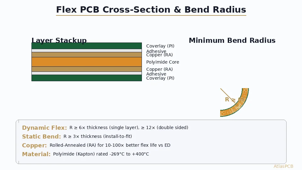
Bend Radius Design Rules
Static vs. Dynamic Bend Classification
Static bend (install and forget): The flex section is bent once during assembly and remains in that position for the product lifetime. Examples: folded PCBs in smartphones, bent connections between stacked boards in medical devices.
Dynamic bend: The flex section bends repeatedly during normal operation. Examples: laptop hinges, printer heads, robotic cable assemblies, automotive door connections.
The classification determines the minimum bend radius:
| Application | Single-Sided Flex | Double-Sided Flex |
|---|---|---|
| Static (one-time bend) | 6× flex thickness | 6× flex thickness |
| Dynamic (≤ 1,000 cycles) | 10× flex thickness | 15× flex thickness |
| Dynamic (≤ 100,000 cycles) | 12× flex thickness | 20× flex thickness |
| Dynamic (> 100,000 cycles) | 15× flex thickness | 25× flex thickness |
These ratios are measured to the inside of the bend (concave surface), to the innermost copper layer.
Calculating Flex Section Thickness
The flex section thickness includes all layers within the flexible region:
t_flex = t_substrate + t_copper_layers + t_adhesive + t_coverlay
For a two-layer flex section:
- Polyimide substrate: 1.0 mil
- Adhesive (×2): 0.5 mil × 2 = 1.0 mil
- Copper (×2): 0.5 mil × 2 = 1.0 mil (for ½ oz copper)
- Coverlay (×2): 1.0 mil × 2 = 2.0 mil
Total: 5.0 mil
Minimum static bend radius: 5.0 × 6 = 30 mil (0.76 mm) Minimum dynamic bend radius (100K cycles): 5.0 × 20 = 100 mil (2.54 mm)
Reducing Flex Thickness for Tighter Bends
When the mechanical envelope demands a tighter bend radius, reduce the flex section thickness:
- Use thinner copper: ½ oz (0.7 mil) or ⅓ oz (0.47 mil) instead of 1 oz (1.4 mil)
- Use thinner substrate: 0.5 mil polyimide instead of 1.0 or 2.0 mil
- Minimize the number of flex layers: Single-layer flex wherever possible
- Use adhesiveless constructions: Eliminate adhesive layers by using cast polyimide with deposited copper
Each of these reduces the total flex thickness and proportionally reduces the minimum bend radius, enabling tighter packaging.
For detailed [flex PCB design guidelines]/blog/flex-pcb-design-guidelines/), our dedicated guide covers additional strategies for optimizing flex section geometry.
Material Selection for Bend Zone Reliability
Polyimide Substrate
Polyimide (PI) is the standard substrate material for flex and rigid-flex PCBs due to its:
- Mechanical flexibility — can withstand millions of flex cycles at appropriate strain levels
- Thermal stability — Tg > 350°C, compatible with lead-free soldering
- Chemical resistance — withstands standard PCB processing chemistry
- Dimensional stability — low CTE and moisture absorption compared to alternatives
Common polyimide substrates:
| Product | Thickness Range | Key Properties |
|---|---|---|
| Standard PI | 0.5–5.0 mil | Good all-around performance |
| High-modulus PI | 0.5–3.0 mil | Better dimensional stability, stiffer |
| Thin PI (adhesiveless) | 0.5–1.0 mil | Thinnest possible construction, best for dynamic flex |
For [dynamic flex applications]/blog/dynamic-flex-pcb-design-bend-radius-reliability/), adhesiveless polyimide substrates with cast or sputtered copper provide the best fatigue life because they eliminate the adhesive layer — a common failure initiation point.
Copper Types for Flex
The copper type is the single most important material choice for bend zone reliability:
Rolled Annealed (RA) Copper:
- Manufactured by rolling copper ingots into thin foils
- Grain structure is elongated and aligned in the rolling direction
- Superior ductility and fatigue resistance
- Can withstand 10–100× more flex cycles than ED copper
- Preferred for all dynamic flex applications
- Available in ½ oz, ⅓ oz, and thinner
Electrodeposited (ED) Copper:
- Manufactured by electroplating copper onto a rotating drum
- Grain structure is columnar (perpendicular to the foil surface)
- Lower ductility and fatigue resistance
- Adequate for static bend applications
- Less expensive than RA copper
- Standard for rigid PCB layers
High-Ductility ED (HD-ED) Copper:
- Modified electrodeposition process producing finer grain structure
- Performance between standard ED and RA copper
- Suitable for limited dynamic flex (≤ 10,000 cycles)
- Cost between standard ED and RA
Adhesive Systems
The adhesive bonding layers in the flex section affect both reliability and processing:
Acrylic adhesive:
- Excellent flexibility and peel strength
- Good moisture resistance
- Lower Tg (approximately 80–100°C) — may not withstand high-temperature processing
- Preferred for dynamic flex due to superior flexibility
Epoxy adhesive:
- Higher Tg (approximately 150–180°C) — better thermal stability
- Good chemical resistance
- Slightly less flexible than acrylic
- Preferred for static flex applications and high-temperature environments
No adhesive (adhesiveless):
- Copper is deposited directly on polyimide via sputtering and plating
- Eliminates the weakest layer in the flex construction
- Thinnest possible construction
- Best fatigue performance
- Higher cost
Coverlay vs. Flexible Solder Mask
The protective layer in the bend zone must be able to flex without cracking:
Coverlay (polyimide film with adhesive):
- Excellent flexibility — follows the substrate through millions of flex cycles
- Applied by lamination
- Openings are mechanically punched or laser cut
- Preferred for all bend zones, especially dynamic applications
- Registration accuracy: ±3–5 mil (less precise than solder mask)
Flexible solder mask:
- Applied by screen printing or inkjet, like rigid board solder mask
- Better registration accuracy for fine features: ±1–2 mil
- Limited flex life — will crack after 1,000–10,000 flex cycles
- Acceptable only for static bend zones with large bend radii
- Lower cost than coverlay
For bend zones that must survive dynamic flexing, coverlay is the only appropriate choice. Use flexible solder mask only in the rigid sections and in static flex areas where fine feature registration is critical.
Rigid-to-Flex Transition Design
Stress Concentration at the Boundary
The rigid-to-flex transition is the highest-stress area of the entire rigid-flex PCB. The abrupt change in stiffness at the boundary creates a stress concentration that amplifies bending forces.
Design features to reduce stress concentration:
Tapered rigid section: Gradually reduce the rigid section thickness approaching the flex zone by removing copper layers progressively over a 50–100 mil transition region.
Stiffener relief: If a stiffener is used on one side of the flex, taper its edge rather than having a sharp termination.
Coverlay extension: Extend the coverlay into the rigid section by at least 50 mil to provide additional support at the transition.
No abrupt material changes: Avoid placing components, pads, or plated features right at the rigid-flex boundary. Maintain a keepout zone of at least 50 mil on both sides of the boundary.
Conductor Transition Rules
How conductors are routed through the rigid-to-flex transition significantly impacts reliability:
Stagger trace entries: Do not align all conductors at the same point along the rigid-flex boundary. Stagger the entry points so that traces enter the flex zone at different positions along the boundary. This distributes the stress concentration rather than creating a single failure line.
Perpendicular entry preferred: Route traces perpendicular to the rigid-flex boundary wherever possible. Traces that enter at an angle experience uneven stress distribution across their width.
Gradual width transitions: If trace width changes between the rigid and flex sections (common when different copper weights are used), taper the transition over at least 10× the trace width.
Teardrop pads: Add teardrop-shaped pad entries at any pad or via near the rigid-flex boundary. The teardrop distributes stress around the pad-trace junction, preventing crack initiation at this stress concentration point.
Plated Through-Hole Restrictions
Plated through-holes (PTH) in the flex section create rigid columns that cannot flex with the surrounding material. The result is extreme stress concentration at the hole barrel edges during bending, leading to cracking.
Rules for PTH in and near bend zones:
- Never place PTH in the bend zone itself — this is an absolute rule for dynamic flex
- Minimum distance from bend: Place PTH at least 50 mil (1.27 mm) from the edge of the bend zone for static applications
- Use button plating: If vias must exist near the flex area, use button plating (plating only the pad area, not through the full hole) to maintain some flexibility
- Through-hole alternatives: Use conductive adhesive, Z-axis connections, or flex-specific interconnect methods instead of PTH where connections are needed in or near the bend zone
For comprehensive via strategies in rigid-flex designs, see our guide on [via types]/blog/pcb-via-types-guide/).
Manufacturing Considerations
Layer Registration in the Transition Zone
The rigid-to-flex transition requires precise alignment between the rigid multilayer section and the flex layers that continue through both regions. Registration challenges include:
- Different material CTEs — rigid FR-4 and flexible polyimide expand differently during lamination
- Resin flow variation — adhesive squeeze-out at the transition can shift flex layers
- Tooling holes — must be placed in dimensionally stable regions, not in or near flex areas
PCB manufacturers with rigid-flex experience use specialized tooling and registration methods to achieve ±2–3 mil layer alignment in the transition zone.
Controlled Depth Routing
The rigid section must be routed (cut) precisely to the depth where the flex section begins, without damaging the flex layers. This controlled-depth routing requires:
- Z-axis accuracy: ±2 mil depth control
- Material thickness knowledge: Precise measurement of the flex layer position within the stackup
- No flex layer damage: The routing bit must stop above the first flex layer without penetrating it
Some designs use a bookbinder approach where the rigid layers are laminated as separate sub-assemblies (rigid caps) bonded to a continuous flex core, avoiding the need for controlled-depth routing altogether.
Bend Zone Inspection
After fabrication, inspect bend zones for:
- Coverlay adhesion: No delamination, lifting, or bubbling at the coverlay edges
- Copper integrity: No cracks visible under 40× magnification in the transition zone
- Dimensional accuracy: Bend zone length and position match the design within ±5 mil
- Cleanliness: No residues or contaminants trapped under the coverlay
Cross-sectional analysis of representative samples should verify:
- Copper grain structure is consistent (RA copper grain orientation)
- No voids in adhesive layers
- Coverlay-to-substrate bond is continuous
- Conductor spacing is maintained through the transition
Lifecycle Testing and Qualification
IPC-6013 Requirements
IPC-6013 (Qualification and Performance Specification for Flexible/Rigid-Flexible Printed Boards) defines the testing requirements for rigid-flex PCBs. The specification classifies boards into three performance classes:
- Class 1 — General electronic products
- Class 2 — Dedicated service electronic products
- Class 3 — High-performance/harsh environment electronic products
Each class has different requirements for bend testing, thermal cycling, and electrical testing. Class 3, used for medical, military, and aerospace applications, has the most stringent requirements.
Flex Endurance Testing
Per IPC-TM-650, Method 2.4.3:
- Setup: The flex section is clamped in a flex testing machine that bends it through the specified radius
- Bend rate: Typically 10–30 cycles per minute
- Monitoring: Electrical continuity is monitored throughout testing. A resistance increase of more than 10% constitutes failure.
- Pass criteria: The sample must survive the specified number of cycles without open circuits
Required cycle counts by application:
| Application Class | Minimum Flex Cycles |
|---|---|
| Static (install-to-fit) | 1–3 cycles to minimum bend radius |
| Limited dynamic | 1,000–10,000 cycles |
| Standard dynamic | 100,000 cycles |
| High-cycle dynamic | 1,000,000+ cycles |
Thermal Cycling
Thermal cycling tests the combined effects of material CTE mismatch and thermal fatigue:
- Temperature range: -40°C to +85°C (Class 2) or -55°C to +125°C (Class 3)
- Cycle count: 100–1,000 cycles depending on application
- Dwell time: 15–30 minutes at each extreme
- Transition rate: 10–15°C per minute maximum
The rigid-to-flex transition is particularly vulnerable to thermal cycling because the different materials (FR-4, polyimide, adhesive, copper) expand and contract at different rates, creating cyclic stress at the interface.
Peel Strength Testing
Coverlay adhesion in the bend zone is tested per IPC-TM-650, Method 2.4.9:
- Pull rate: 50 mm/minute
- Peel angle: 90° or 180°
- Minimum peel strength: 4 lb/in (700 N/m) for Class 2, 6 lb/in (1,050 N/m) for Class 3
Loss of peel strength after thermal cycling or humidity exposure indicates adhesive degradation that will lead to field failures.
For comprehensive [PCB reliability testing]/blog/pcb-reliability-testing/) methods, our guide covers additional test protocols relevant to rigid-flex qualification.
Cross-Section Analysis
Destructive cross-sectional analysis of the bend zone reveals:
- Microcracking: Cracks in copper traces or plating that are not detectable by electrical testing but will propagate to failure under continued stress
- Delamination initiation: Microscopic separations between layers that indicate adhesive failure
- Copper grain structure: Verification that RA copper was used (elongated grains) and not inadvertently substituted with ED copper (columnar grains)
- Dimensional compliance: Actual layer thicknesses, trace widths, and spacings match the design
Best Practices Summary
Design Rules Checklist
- Bend radius meets minimum ratio for the application type (static/dynamic)
- Flex section thickness is minimized (thin copper, thin substrate, minimal layers)
- Conductors are staggered at the rigid-flex transition
- No plated through-holes in the bend zone
- Teardrop pads at all features near the transition boundary
- Keepout zone of ≥ 50 mil on both sides of the rigid-flex boundary
- Coverlay (not flexible solder mask) used in bend zones
- Copper type specified (RA for dynamic, ED acceptable for static only)
- Stress relief features at the rigid-to-flex transition (tapers, radiused corners)
- [DFM verification]/blog/pcb-dfm-checklist/) completed for the rigid-flex-specific manufacturing steps
Material Specification
For dynamic rigid-flex bend zones, specify:
- Substrate: Adhesiveless polyimide, 0.5–1.0 mil
- Copper: Rolled annealed, ½ oz or thinner
- Coverlay: Polyimide with acrylic adhesive
- Rigid section: Standard FR-4 or [high-Tg material]/blog/high-tg-pcb-material-selection/) as required by the application
- Bonding adhesive: Acrylic for dynamic, epoxy for static
Design for Test
Include test features in the design:
- Daisy-chain patterns through the bend zone for continuity monitoring during flex testing
- Dedicated test coupons on the production panel that can be sectioned for cross-section analysis
- Resistance measurement pads at both ends of critical bend zone conductors for in-circuit testing
Conclusion
Bend zone reliability is not a matter of luck — it is a matter of engineering. Every aspect of the design, from bend radius to copper type to transition geometry, directly impacts whether the product will survive its intended service life.
The most common bend zone failures trace back to three root causes:
- Insufficient bend radius for the application type (the most common error)
- Wrong copper type — using ED copper in dynamic applications
- Stress concentration at the rigid-flex transition — sharp boundaries, untapered stiffeners, or PTH in the bend zone
All three are preventable through proper design practice. Apply the rules in this guide, specify the right materials, and validate with appropriate testing — and your rigid-flex bend zones will perform reliably throughout the product lifecycle.
Ready to design a reliable rigid-flex PCB?
Upload your Gerbers for a free engineering review — our rigid-flex specialists will evaluate your bend zone design, material selection, and transition geometry for optimal reliability. Get a quote today →
Further Reading
- [PCB Design for GaN and SiC Power Devices: Thermal Management, Layout Rules, and Material Selection]/blog/pcb-design-gan-sic-power-devices-thermal-layout/)
- [Dynamic Flex PCB Design — Bend Radius, Material Selection, and Reliability]/blog/dynamic-flex-pcb-design-bend-radius-reliability/)
- [PCB Panelization and Array Design: V-Score vs Tab Routing, DFM Rules, and Cost Optimization]/blog/pcb-panelization-v-score-tab-routing-dfm-cost-optimization/)
- [mmWave PCB Material Selection: Rogers vs Megtron vs LCP for 5G and 6G Applications]/blog/mmwave-pcb-material-selection-rogers-megtron-lcp-5g-6g/)
- [Rogers PCB Fabrication: Material Sourcing, Lead Times & Quality Control]/blog/rogers-pcb-fabrication/)
- Our Manufacturing Capabilities
About AtlasPCB — We specialize in complex PCB manufacturing for HDI, RF, and high-reliability applications. Explore our rigid-flex PCB manufacturing . Every order includes free engineering review. Get your quote.
Reviewed by AtlasPCB Engineering Team — IPC-certified manufacturing specialists with 15+ years of production experience in HDI, RF, and high-reliability PCB fabrication. Content based on factory floor data and real customer design reviews.
- rigid-flex
- bend-zone
- reliability
- flex-pcb
- lifecycle-testing