· AtlasPCB Engineering · Engineering · 10 min read
Flex PCB Design Guidelines: Bend Radius, Conductor Routing, Stiffeners, and Material Selection
Comprehensive design guidelines for flexible printed circuits (FPC) covering bend radius calculations, conductor routing rules, stiffener design, material selection, and reliability considerations for single-layer, double-layer, and multilayer flex circuits.
Flexible printed circuits (FPC) enable designs that rigid PCBs cannot—folding, bending, continuous flexing in hinges, and conforming to non-planar shapes. However, designing a flex circuit that survives assembly and service life requires understanding the unique rules of flex design. This guide covers the critical design parameters for reliable flex circuits.
Flex PCB Types
Single-Layer Flex
One copper conductor layer on a polyimide substrate, covered by a polyimide coverlay. The simplest and most flexible construction.
- Typical thickness: 0.05–0.15 mm
- Applications: Ribbon cables, LED strips, camera modules, sensor connections
- Cost: Lowest
Double-Layer Flex
Two copper layers with polyimide dielectric between them and coverlay on both sides. Plated through-holes connect the layers.
- Typical thickness: 0.10–0.25 mm
- Applications: Smartphone flex cables, hard drive head assemblies, medical devices
- Cost: Moderate
Multilayer Flex
Three or more copper layers with polyimide dielectrics. Can include plated through-holes and blind vias.
- Typical thickness: 0.15–0.50 mm
- Applications: Military avionics, satellite systems, high-density portable electronics
- Cost: High
Rigid-Flex
Combines rigid PCB sections (FR-4) with flexible sections (polyimide). The flex sections are integrated into the multilayer stackup during lamination—not attached afterward. For comprehensive rigid-flex design guidance, see our [rigid-flex PCB design guide]/blog/rigid-flex-pcb-design/).
- Typical thickness: Rigid: 0.8–2.0 mm; Flex: 0.1–0.3 mm
- Applications: Aerospace, medical implants, military electronics, consumer devices (wearables, folding phones)
- Cost: Highest
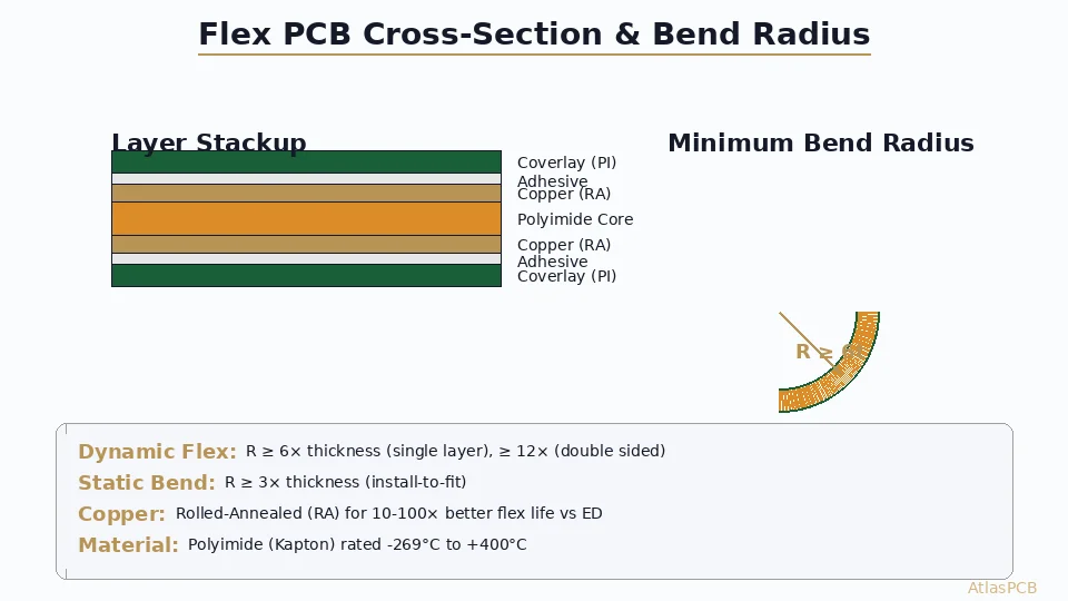
Bend Radius
The minimum bend radius is the most critical parameter in flex PCB design. Too tight a bend overstresses the copper conductors, leading to cracking and failure.
Bend Radius Calculation
The minimum bend radius depends on:
- Total flex thickness (t): Including all copper layers, dielectric, coverlay, and adhesive
- Number of copper layers: More layers = stiffer = larger minimum radius
- Flex type: Dynamic (repeated bending) vs. static (one-time bend)
- Copper type: Rolled annealed (RA) vs. electrodeposited (ED)
- Number of flex cycles: More cycles require larger radius
Recommended Minimum Bend Radius
| Flex Type | Application | Min Bend Radius | Notes |
|---|---|---|---|
| Single-layer, static | Install and forget | 3 × t | RA copper recommended |
| Single-layer, dynamic | <100K cycles | 6 × t | RA copper required |
| Single-layer, dynamic | >100K cycles | 10 × t | RA copper, no plating in flex area |
| Double-layer, static | Install and forget | 5 × t | Use bookbinder construction |
| Double-layer, dynamic | <100K cycles | 10 × t | Stagger conductors |
| Double-layer, dynamic | >100K cycles | 15 × t | Special design considerations |
| Multilayer, static | Install and forget | 10 × t | Minimize layers in flex zone |
| Rigid-flex transition | Static | 6 × t_flex | Taper transition zone |
Example calculation:
Single-layer flex circuit:
- Polyimide base: 25 µm
- Adhesive: 15 µm
- Copper (1/2 oz): 18 µm
- Coverlay adhesive: 15 µm
- Coverlay film: 25 µm
- Total thickness (t): 98 µm ≈ 0.1 mm
Dynamic bend radius (6× rule): 6 × 0.1 mm = 0.6 mm minimum
Neutral Axis Design
When a flex circuit bends, the outer surface stretches and the inner surface compresses. The neutral axis is the plane within the circuit that experiences zero strain. Positioning the copper conductors at or near the neutral axis minimizes stress during bending.
For single-layer flex: The neutral axis is approximately at the center of the total thickness. Since there is only one copper layer, it cannot be centered perfectly—but using symmetric coverlay (same material and thickness on both sides) helps.
For double-layer flex (bookbinder construction): Instead of bonding two layers together with adhesive (which puts copper on the outer surfaces), the two layers are left unbonded in the flex zone. Each layer bends independently around its own neutral axis, dramatically improving flex life. The layers are bonded in the rigid/pad areas only.
For multilayer flex: Place copper layers as close to the neutral axis as possible. Avoid placing copper on the outermost layers in the flex zone.
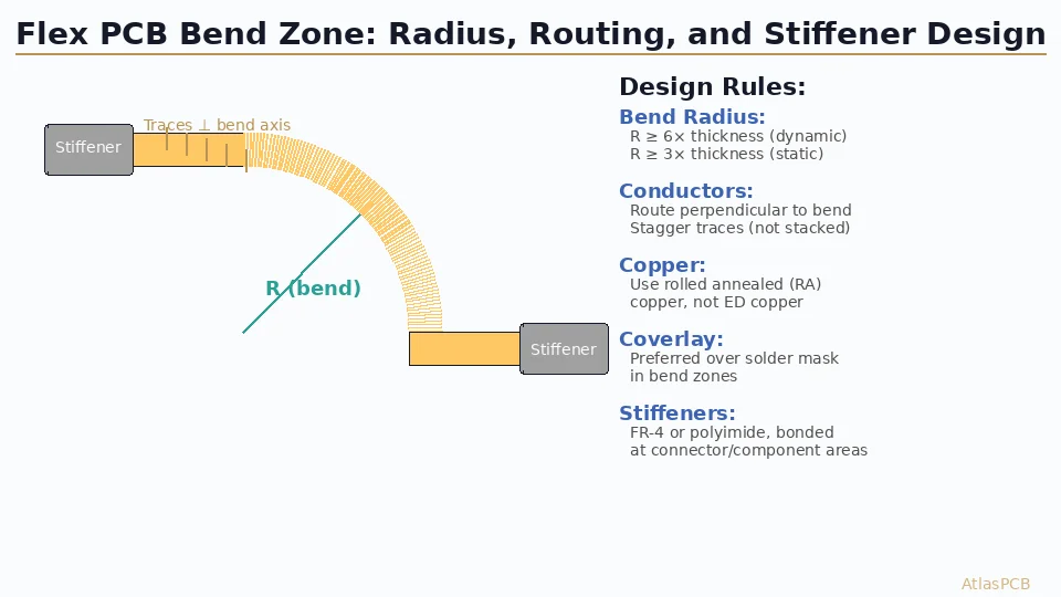
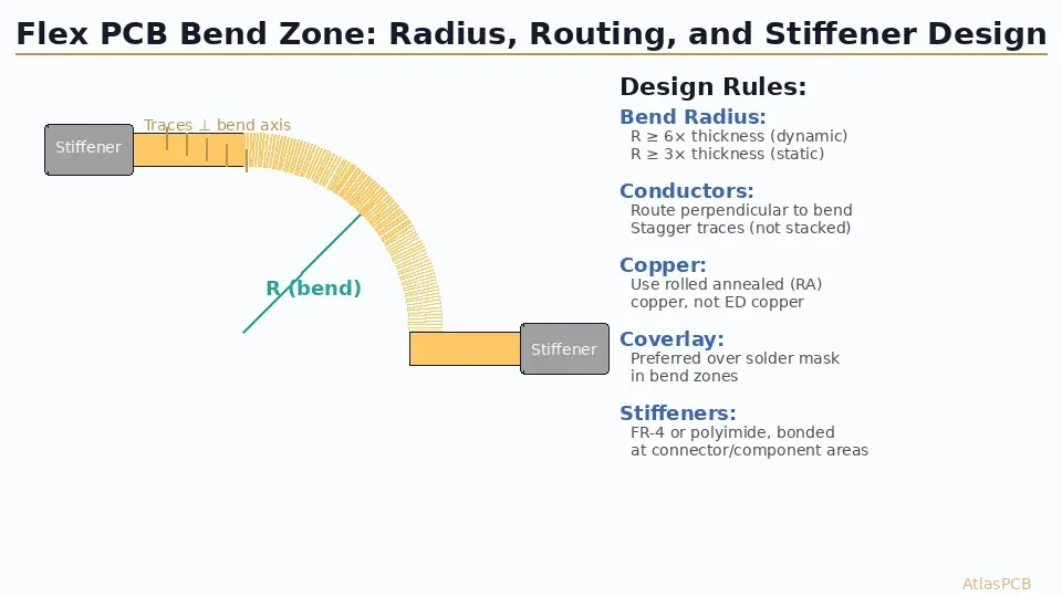
Conductor Routing in Flex Areas
Route Perpendicular to Fold Line
Conductors should cross the bend axis at right angles (perpendicular to the fold line). Conductors running parallel to the fold line experience maximum strain during bending and are much more likely to crack.
If angled routing is unavoidable, keep the angle ≥45° to the fold line.
Stagger Conductors on Multi-Layer Flex
On double-layer flex circuits, do NOT align conductors on Layer 1 directly above conductors on Layer 2. Instead, stagger them so that each conductor on one layer falls between conductors on the other layer. This creates a more uniform cross-section and reduces localized stress points.
Avoid Sharp Corners in Flex Areas
Conductors in the flex zone should not have abrupt direction changes. Use smooth curves with radius ≥0.5 mm. Sharp corners create stress concentration points that initiate cracks during bending.
Conductor Width and Spacing
In the flex zone, traces should be as wide as possible (within routing constraints) and evenly spaced:
| Parameter | Minimum (standard) | Recommended |
|---|---|---|
| Trace width in flex zone | 75 µm (3 mil) | ≥100 µm (4 mil) |
| Trace spacing in flex zone | 75 µm (3 mil) | ≥100 µm (4 mil) |
| Trace-to-edge clearance | 250 µm (10 mil) | ≥500 µm (20 mil) |
No Plated Through-Holes in Dynamic Flex Areas
Plated through-holes are rigid points that create stress concentration during bending. Never place vias in a dynamic flex zone. For static bends, vias can be present but should be at least 1.0 mm from the bend tangent point.
Copper Type: RA vs. ED
Rolled Annealed (RA) copper has an elongated grain structure parallel to the rolling direction, providing superior flex endurance (10–100× more flex cycles than ED copper). Always specify RA copper for flex zones.
Electrodeposited (ED) copper has a columnar grain structure perpendicular to the surface. It is stiffer and more prone to cracking during bending. Use ED copper only in rigid areas where cost is a priority.
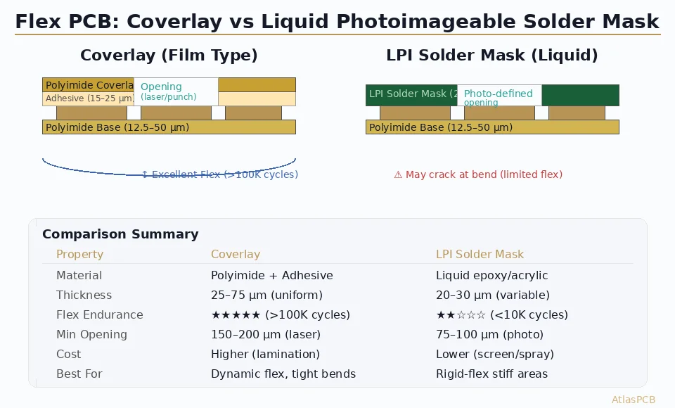
Coverlay and Cover Films
Polyimide Coverlay
The standard protection for flex circuits:
- Material: Polyimide film (12.5 or 25 µm) with acrylic or epoxy adhesive (12.5 or 25 µm)
- Total thickness: 25–50 µm
- Advantages: Excellent chemical resistance, high temperature capability, good flex endurance
- Patterning: Mechanical punch or laser cut for pad openings
- Limitations: Limited minimum opening size (~200 µm) and position accuracy (±75 µm) compared to solder mask
Flexible Solder Mask
For fine-pitch components on flex circuits:
- Material: Liquid photoimageable (LPI) flexible solder mask
- Thickness: 10–25 µm
- Advantages: Finer features (75 µm openings), better positional accuracy (±25 µm), lower profile
- Limitations: Less chemical resistant than coverlay, shorter flex life in dynamic applications, not suitable for tight bend radii
Design Rules for Coverlay
- Minimum dam width: 200 µm (coverlay), 100 µm (flex solder mask)
- Minimum opening: 200 µm (coverlay), 100 µm (flex solder mask)
- Coverlay-to-pad clearance: 75–125 µm per side (larger than solder mask registration)
- Extension beyond conductors: Coverlay should extend ≥250 µm beyond the edge of conductor patterns
Stiffeners
Stiffeners provide local rigidity where components are mounted or mechanical attachment is needed.
Stiffener Materials
| Material | Thickness | Attachment | Application |
|---|---|---|---|
| FR-4 | 0.2–1.6 mm | PSA or thermal bond | Component areas, connector areas |
| Polyimide | 0.1–0.5 mm | PSA or thermal bond | Thin stiffening, ZIF connector area |
| Stainless steel | 0.1–0.3 mm | PSA | EMI shielding + stiffening, grounding |
| Aluminum | 0.3–1.0 mm | PSA or thermal bond | Heat spreading + stiffening |
Stiffener Design Rules
- Stiffener placement: Must extend ≥2.0 mm beyond the outermost component pad in all directions
- Transition zone: Taper the stiffener edge or add a gradual thickness transition to avoid a sharp bend point at the stiffener boundary
- Adhesive selection: PSA (pressure-sensitive adhesive) for low-temperature applications; thermal-cure adhesive for reflow-surviving bonds
- Assembly sequence: Stiffeners are typically applied before SMT assembly. Verify that the stiffener’s total added height does not interfere with the reflow profile or pick-and-place equipment.
- ZIF connector stiffeners: Must provide 0.2–0.3 mm total thickness at the insertion tab (check connector specification). FR-4 or polyimide stiffener is typically bonded to the back side.
Material Selection
Base Dielectric
| Material | Dk (1 GHz) | Flex Endurance | Temperature | Cost |
|---|---|---|---|---|
| Polyimide (Kapton HN) | 3.4 | Excellent | -269 to +400°C | Baseline |
| Polyester (PET/Mylar) | 3.2 | Good | -60 to +105°C | 0.5× |
| LCP (Liquid Crystal Polymer) | 2.9 | Good | -50 to +280°C | 2× |
| PTFE (Teflon) | 2.1 | Fair | -200 to +260°C | 3× |
Polyimide is the default choice for nearly all flex PCB applications due to its combination of flex endurance, temperature resistance, and chemical compatibility.
Polyester (PET) is used for low-cost, low-temperature applications (consumer electronics with minimal flex requirements).
LCP is emerging for high-frequency flex applications (5G antenna feeds, mmWave flexible interconnects) due to its low Dk and Df.
Adhesive Systems
- Acrylic adhesive: Traditional, good flex endurance, Tg ~45°C (soft at room temperature), limited high-temperature performance
- Epoxy adhesive: Better high-temperature performance, Tg >120°C, slightly less flexible
- Adhesiveless (cast polyimide): Best flex endurance and reliability, thinnest construction, highest cost. Preferred for dynamic flex applications.
Copper Foil
| Type | Grain Structure | Flex Endurance | Min Thickness | Application |
|---|---|---|---|---|
| Rolled Annealed (RA) | Elongated (parallel to surface) | Excellent (MIT 200+ folds) | 9 µm (¼ oz) | Dynamic flex zones |
| Electrodeposited (ED) | Columnar (perpendicular to surface) | Poor-Fair (MIT 10-50 folds) | 9 µm (¼ oz) | Rigid areas only |
| High-ductility ED | Modified columnar | Good (MIT 50-100 folds) | 12 µm (⅓ oz) | Moderate flex zones |
Design for Manufacturing (DFM) Guidelines
Panel Layout
- Flex orientation: Align flex circuits so that the machine direction (MD) of the copper foil is perpendicular to the fold line (RA copper has best flex endurance when bent perpendicular to the rolling direction)
- Panel utilization: Flex panels are typically polyimide (more expensive than FR-4). Optimize panelization for maximum yield.
- Registration: Flex materials are less dimensionally stable than FR-4. Allow for ±100 µm registration tolerance vs. ±50 µm for rigid PCB.
Pad Design
- Anchor pads: Increase pad area in flex zones by adding copper anchors (teardrops) at pad-to-trace junctions. This reinforces the weak point where a narrow trace meets a larger pad.
- Annular ring: Minimum 125 µm for through-hole pads (vs. 75 µm for rigid)
- Via pads: 1.5× drill diameter minimum (vs. 1.3× for rigid)
Outline and Routing
- Minimum feature size: Internal cutouts ≥1.0 mm radius corners (stress concentration at sharp internal corners)
- Tab connections: Use curved tabs connecting the flex to the panel frame; straight tabs with sharp corners initiate tears
- Edge chamfer: Chamfer or radius all external corners to prevent crack initiation
Reliability Testing for Flex
MIT Fold Endurance (IPC-TM-650 2.4.3)
The MIT folding endurance test measures how many 180° bends a flex circuit (or material sample) can withstand before conductor failure:
- Test conditions: 135° fold (equivalent), 0.5 kg tension, 175 cycles per minute
- Typical results: RA copper on adhesiveless polyimide: 200–500+ cycles; ED copper: 10–50 cycles
Flex Cycle Testing
For dynamic flex applications:
- Build representative test samples with actual circuit routing
- Mount in a flex cycling fixture at the design bend radius
- Cycle at the expected flex rate (typically 1–30 Hz)
- Monitor electrical continuity
- Run to target cycle count + 50% safety margin
Thermal Cycling
Flex circuits in automotive and aerospace applications must survive thermal cycling:
- Automotive: -40°C to +125°C, 1000 cycles
- Aerospace: -55°C to +125°C, 500 cycles
- Verify coverlay adhesion, solder joint integrity, and conductor continuity after cycling
Common Flex Design Mistakes
- Running traces parallel to the fold line — most common cause of field failures
- Using ED copper in flex zones — dramatically reduced flex life
- Placing vias in or near the flex zone — creates stress risers
- No transition zone between rigid and flex — sudden thickness change creates a crack initiation point
- Symmetric trace arrangement on double-layer flex — traces directly above each other create I-beam stiffness instead of staggered arrangement
- Tight bend radius without calculating total thickness — forgetting to include coverlay and adhesive in the thickness calculation
- No stiffener in component areas — leads to solder joint cracking during assembly or service
- Ignoring copper grain direction — RA copper flex endurance is directional; bend axis must be perpendicular to grain direction
Conclusion
Flex PCB design requires a fundamentally different mindset from rigid PCB design. Bend radius, conductor orientation, material selection, and stiffener design all interact to determine whether a flex circuit will survive assembly and field use. Following the guidelines in this article—combined with early DFM review from your fabricator—significantly reduces the risk of flex design failures.
At Atlas PCB, we manufacture single-layer, double-layer, multilayer flex, and rigid-flex PCBs in our advanced flex fabrication facility. Our engineering team provides DFM feedback specific to your flex design’s bend requirements and material needs. Get a quote for your flex PCB project.
For related reading, explore our [rigid-flex PCB design guide]/blog/rigid-flex-pcb-design/) and our general [PCB design rules guide]/blog/pcb-design-rules-trace-width-spacing/).
Further Reading
- [Blind Via vs Buried Via: Design Rules, Cost Impact & When to Use Each]/blog/blind-via-vs-buried-via/)
- [PCB DFM Checklist: 50 Points to Review Before Sending Gerbers]/blog/pcb-dfm-checklist/)
- [PCB Solder Mask: Types, Colors, and Functions Explained]/blog/pcb-solder-mask-guide/)
- [EMC/EMI Design for PCBs: Passing Compliance on the First Try]/blog/emc-emi-pcb-design/)
About AtlasPCB — We specialize in complex PCB manufacturing for HDI, RF, and high-reliability applications. Explore our rigid-flex PCB manufacturing . Every order includes free engineering review. Get your quote.
Reviewed by AtlasPCB Engineering Team — IPC-certified manufacturing specialists with 15+ years of production experience in HDI, RF, and high-reliability PCB fabrication. Content based on factory floor data and real customer design reviews.
- flex PCB
- FPC
- bend radius
- polyimide
- stiffener
- flexible circuit