· AtlasPCB Engineering · Engineering · 12 min read
PCB Design for AI Edge Inference: Thermal, Power Delivery, and Signal Integrity Challenges
Engineering guide for PCB designers building AI edge inference hardware. Covers thermal management for NPUs, power delivery network design for transient AI workloads, and high-speed memory interface routing for edge ML accelerators.
The Edge AI PCB Design Challenge
Edge AI inference is fundamentally different from data center AI in ways that directly impact PCB design decisions. Where a data center GPU board has 400W thermal design power spread across a large card with forced-air cooling and redundant power supplies, an edge inference module must dissipate 10-25W in a form factor the size of a credit card, often with passive cooling or limited airflow, powered by a single voltage rail from a battery or compact supply.
This concentration of computational power into small, thermally constrained packages creates engineering challenges that transcend traditional embedded system design. The NPU (Neural Processing Unit) devices entering the market from Qualcomm, MediaTek, Hailo, Kneron, and others pack dense matrix multiply engines into 8x8mm to 15x15mm packages, producing localized power densities of 10-20 W/cm2 — comparable to laptop processors but without laptop-class thermal solutions.
The PCB becomes simultaneously the structural platform, thermal pathway, power distribution network, and signal transmission medium. Compromising any of these functions to optimize another creates a design that either overheats, drops voltage during inference bursts, or fails to maintain data integrity at multi-gigabit memory interfaces. The solution requires a holistic approach to stackup design, material selection, and layout strategy that balances all four requirements.
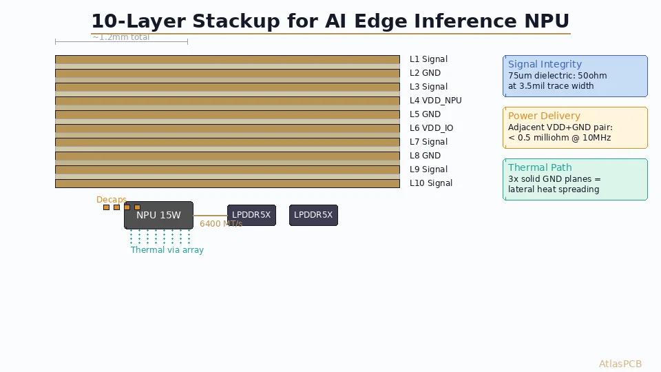
Stackup Architecture for Edge NPU Designs
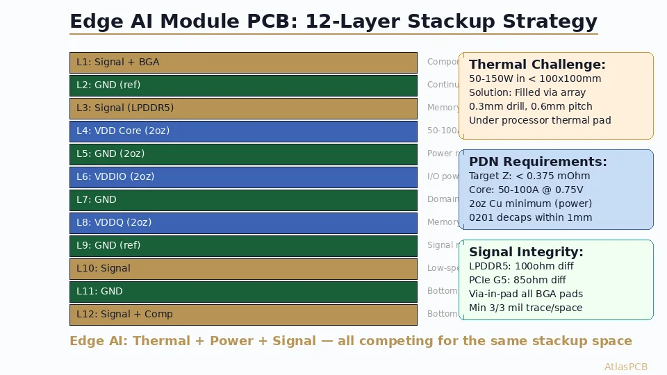
The stackup is the foundation of every design decision that follows. For edge AI boards, the stackup must accomplish four things simultaneously: provide low-impedance power delivery, establish solid reference planes for high-speed memory interfaces, create thermal pathways from the NPU to the board surface, and route all signals within the available area.
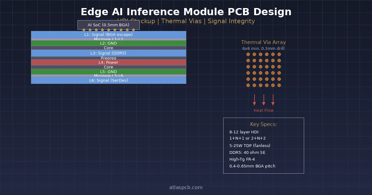
A production-proven 10-layer stackup for a typical edge NPU with LPDDR5X memory follows this general structure:
| Layer | Function | Material/Thickness | Notes |
|---|---|---|---|
| L1 | Signal (NPU breakout + components) | 35um Cu + 75um prepreg | NPU BGA fanout, decap pads |
| L2 | Ground plane (solid) | 35um Cu | Primary reference for L1 signals |
| L3 | Signal (memory interface) | 18um Cu + 100um core | LPDDR5X DQ/DQS routing |
| L4 | Power plane (VDD_NPU) | 35um Cu + 100um prepreg | Low-impedance core supply |
| L5 | Ground plane (solid) | 35um Cu + 100um core | PDN return, thermal spreading |
| L6 | Power plane (VDD_IO + VDD_MEM) | 35um Cu + 100um prepreg | Split plane for I/O domains |
| L7 | Signal (peripheral routing) | 18um Cu + 100um core | USB, UART, SPI, GPIO |
| L8 | Ground plane (solid) | 35um Cu | Reference for L7 and L9 |
| L9 | Signal (power supply routing) | 18um Cu + 75um prepreg | Inductor-to-capacitor routes |
| L10 | Signal + ground pour | 35um Cu | Bottom components, thermal pad |
This structure provides three solid ground planes (L2, L5, L8) that serve as both signal references and thermal spreading layers. The 75um prepreg between L1 and L2 achieves 50-ohm single-ended impedance at 3.5mil trace width on standard FR-4, which fits within the NPU BGA pitch constraints (0.4-0.5mm pitch typical for edge NPUs).
The key insight is that ground planes in an edge AI design do triple duty: signal reference, PDN return current path, and thermal conduction. Every slot, split, or cutout in a ground plane degrades all three functions simultaneously. Design ground planes as unbroken copper sheets with zero routing exceptions — route all signals on dedicated signal layers, never on ground or power layers.
HIGH-DENSITY PCB FOR AI EDGE
8-12 Layer HDI With Fine-Pitch BGA Breakout
Laser-drilled microvias, 75um trace/space, and impedance-controlled stackups for NPU and LPDDR5X interfaces.
Get Stackup Review ›Thermal Management: Designing for Burst Power
Edge NPU thermal behavior is unlike traditional continuous-power processors, and this distinction demands a different design approach. A typical edge inference workload consists of short burst periods (10-50ms of intense computation at 15-25W) followed by idle periods (50-500ms at 2-3W). The NPU junction temperature ramps rapidly during each burst, limited primarily by the thermal capacitance of the die and package, then cools partially during idle.
This thermal cycling pattern has two consequences for PCB design. First, the steady-state average power (perhaps 5-8W) is misleading — the PCB thermal design must handle peak power or the junction temperature will exceed limits during sustained burst sequences. Second, the repetitive thermal cycling fatigues solder joints on the NPU BGA faster than equivalent continuous power would, because the thermal expansion differential between silicon die and PCB substrate cycles thousands of times per day rather than reaching a steady equilibrium.
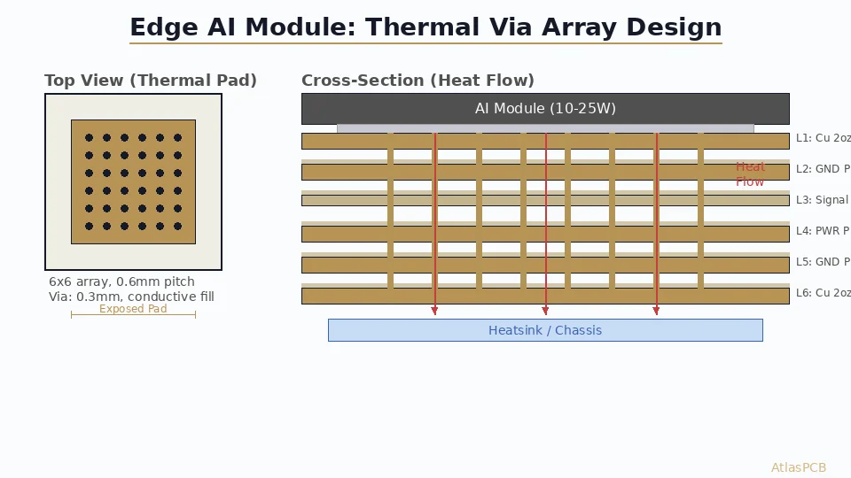
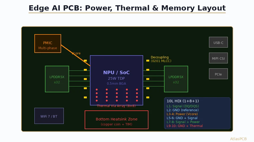
The thermal via array beneath the NPU exposed pad is the primary heat extraction mechanism in passively cooled edge devices. A well-designed via array uses 0.3mm diameter plated through-holes on 0.8mm pitch, filling the entire exposed pad area. For a 10x10mm thermal pad, this yields approximately 144 vias (12x12 array) with an effective thermal resistance of 15-20 C/W from pad top to board bottom. Combined with a copper pour on the bottom layer and either a thermal pad to chassis or convective cooling, this structure handles 15-20W peak power while maintaining junction temperatures below 100C in typical ambient conditions.
Via-in-pad plated over (VIPPO) construction is preferred for NPU thermal pads because it provides a flat, solderable surface above the via array. Standard vias with tented solder mask create air gaps beneath the component that act as thermal insulators, reducing the effectiveness of the via array by 30-50%. VIPPO eliminates these air gaps, ensuring direct copper-to-solder contact across the entire thermal pad area. AtlasPCB produces via-in-pad plated over (VIPPO) as a standard process for BGA and thermal pad applications.
Power Delivery Network for Sub-Nanosecond Transients
The power delivery network (PDN) for an edge NPU core supply is perhaps the most demanding aspect of the PCB design. The NPU core voltage is typically 0.75-0.9V with a tolerance of plus/minus 3% (22-27mV). Peak current draw of 50-80A means the total PDN impedance from VRM output to die must remain below 0.3-0.5 milliohms from DC to the frequency where on-die capacitance takes over (typically 50-100 MHz for edge NPUs).
Achieving sub-milliohm impedance requires several coordinated design elements working together. The power plane pair (VDD + adjacent GND) forms a distributed capacitor with low impedance at high frequencies. At 100um dielectric spacing between planes, FR-4 provides approximately 50pF per square centimeter of interplane capacitance — useful above 200 MHz but insufficient alone to meet the impedance target below that frequency.
Decoupling capacitors bridge the gap between VRM bandwidth (typically below 100 kHz) and the interplane capacitance resonance. For edge NPU PDNs, a three-tier approach is standard: bulk capacitors (22-100uF MLCC, X5R/X7R) placed within 5mm of the NPU for 10 kHz-1 MHz coverage; midband capacitors (0.1-1uF, 0201 or 01005) placed within 2mm of BGA balls for 1-50 MHz coverage; and high-frequency capacitors (10-100nF, 0201 with minimal ESL) placed directly at power ball positions or on the back side beneath the BGA footprint for 50-200 MHz coverage.
The critical layout rule is that every decoupling capacitor’s current loop area must be minimized. A capacitor on L1 with a via down to the VDD plane on L4 and a via to ground on L5 creates a 300um-high loop that adds 200-400pH of inductance per via. This inductance dominates above 50 MHz and can create anti-resonance peaks that violate the impedance target. The solution: place capacitors as close as physically possible to the power ball exits, use multiple vias per capacitor pad to reduce via inductance, and ensure the VDD and GND planes are on adjacent layers with minimum dielectric spacing.
ADVANCED PDN DESIGN SUPPORT
Precision Stackups for High-Current AI Boards
Controlled dielectric thickness to plus/minus 10%. Up to 5oz copper inner layers. Via-in-pad for BGA decoupling.
Upload Design Files ›Memory Interface Routing: LPDDR5X at 6400 MT/s
The memory interface on an AI edge board connects the NPU to one or two LPDDR5X packages operating at up to 6400 MT/s (3200 MHz clock). At these data rates, the PCB trace is not a simple conductor — it is a transmission line where impedance discontinuities, length mismatches, and dielectric loss directly affect the data eye opening at the receiver.
LPDDR5X uses a single-ended signaling scheme with 40-50 ohm characteristic impedance (depending on SoC vendor specification). The DQ (data) and DQS (strobe) signals must be matched in length within a byte lane to within plus/minus 0.5mm (approximately 3.5ps skew at FR-4 propagation speed). Address and command signals have relaxer matching requirements (plus/minus 2mm) because they operate at half the data rate.
The routing strategy for edge devices differs from server boards primarily in trace length. Edge modules typically place memory packages within 5-15mm of the NPU, which is short enough that FR-4 dielectric loss does not significantly close the data eye. At 10mm trace length on standard FR-4 (Df = 0.02), insertion loss at the Nyquist frequency (3.2 GHz for 6400 MT/s) is approximately 0.3 dB — well within margin for LPDDR5X receivers that tolerate 3-4 dB total channel loss.
The bigger challenge on compact edge boards is crosstalk. With 4/4mil (100/100um) trace/space on a thin 75um dielectric, the coupling between adjacent data lines can reach -15 to -20 dB. For byte lanes routed in parallel over distances of 10mm+, this crosstalk aggresses timing jitter equivalent to 5-10% of the data eye width. Mitigation strategies include: routing DQ signals on stripline layers (sandwiched between two ground planes) rather than microstrip, maintaining 2x trace-width spacing between byte lanes, and using ground guard traces between DQ groups heading to different memory packages.
Material Selection: Balancing Cost and Performance
Not every edge AI board requires exotic low-loss laminates. The material selection depends on the specific interface speeds, trace lengths, and margin requirements. Over-specifying materials adds 30-60% to bare board cost without meaningful performance benefit.
Standard FR-4 (IT-180A, S1000-2, EM-285): Adequate for LPDDR5 at 4800 MT/s with trace lengths under 15mm, and for all peripheral interfaces (USB 3.x, PCIe Gen 3, MIPI). Dk 4.2-4.4, Df 0.018-0.022 at 1 GHz. This covers the majority of edge AI designs where the memory is placed close to the NPU on a compact module.
Mid-loss FR-4 (IT-170GRA, EM-370D, Megtron 4): Recommended for LPDDR5X at 6400 MT/s with trace lengths of 10-25mm, and for PCIe Gen 4/5 interfaces with runs over 50mm. Dk 3.8-4.0, Df 0.008-0.012 at 1 GHz. The cost premium over standard FR-4 is typically 20-35% on the bare board, justified when simulation shows standard FR-4 eye closure approaching receiver limits.
Ultra-low-loss (Megtron 6, Megtron 7, Tachyon-100G): Rarely necessary for edge inference boards unless the design includes 112G SerDes interfaces (unlikely in current edge NPUs) or PCIe Gen 6 links. These materials add 60-100% board cost premium and are justified only when loss budget analysis shows mid-loss materials fail. Reserve for data center and networking applications.
For most edge AI modules, a pragmatic approach uses standard FR-4 for all layers except the memory signal layer(s), where a single prepreg layer of mid-loss material between signal and reference plane provides adequate loss performance at minimal cost uplift. This hybrid approach costs only 10-15% more than all-FR-4 while delivering the signal integrity margin where it matters.
HYBRID STACKUP CONSTRUCTION
Mixed-Material Stackups for Cost-Optimized Performance
Combine standard FR-4 with targeted low-loss layers exactly where your signals need them. HDI construction up to 5+N+5 buildup.
HDI Capabilities ›Design Checklist for AI Edge Inference PCBs
Before sending your edge AI board for fabrication, verify these critical items that catch the most common design escapes:
Thermal path continuity: Confirm that thermal vias beneath the NPU connect through all ground planes without being broken by signal routing on inner layers. A single inner-layer trace crossing through the via array can eliminate 10-20% of your thermal via effectiveness by forcing heat to flow around the blockage.
PDN impedance verification: Run a simple parallel-plate impedance calculation (or use a tool like Altium PDN Analyzer or Ansys SIwave) to verify that your target impedance is achievable with the planned capacitor count and placement. The most common failure mode is insufficient mid-band capacitors in the 1-50 MHz range where neither the VRM nor the interplane capacitance provides adequate impedance.
Memory trace length matching: Verify byte-lane matching to plus/minus 0.5mm for DQ-to-DQS within each byte group, and plus/minus 2.0mm for address/command to clock. Use your EDA tool’s matched-length routing function and verify post-route — automatic routers sometimes violate matching on inner layers where visibility is limited.
Impedance stack verification with fabricator: Before committing your design, submit the proposed stackup to your PCB fabricator for impedance modeling. The fabricator’s actual material Dk (which varies from published values by 5-10% depending on resin content and glass style) determines whether your 3.5mil trace achieves 50 ohms or 53 ohms. AtlasPCB provides impedance-controlled fabrication with pre-production stackup modeling to verify target impedance before manufacturing.
ATLASPCB
Building AI Edge Hardware? Let Us Handle the PCB.
From stackup optimization to impedance verification, we fabricate the boards that power edge AI devices. Upload your design for a detailed engineering review and quotation.
Get Instant Quote ›Related Reading:
About AtlasPCB — We specialize in complex PCB manufacturing for HDI, RF, and high-reliability applications. Explore our aluminum and metal-core PCB services . Every order includes free engineering review. Get your quote.
Reviewed by AtlasPCB Engineering Team — IPC-certified manufacturing specialists with 15+ years of production experience in HDI, RF, and high-reliability PCB fabrication. Content based on factory floor data and real customer design reviews.
- AI edge inference
- NPU PCB design
- thermal management
- power delivery network
- edge AI
- ML accelerator
- PCB design