· AtlasPCB Engineering · Engineering · 12 min read
High-Speed Backplane PCB Design: Signal Integrity, Material Selection & Layout Best Practices
Master high-speed backplane PCB design with proven strategies for signal integrity, material selection, impedance control, and differential pair routing in multi-gigabit systems.
Why Backplane PCB Design Demands Specialized Engineering
Backplane printed circuit boards serve as the central nervous system of complex electronic systems — from telecommunications switches and data center routers to defense radar arrays and industrial automation controllers. Unlike standard daughter cards, a backplane must reliably route hundreds or even thousands of high-speed signals across distances of 500 mm or more while maintaining signal integrity at data rates that now routinely exceed 25 Gbps per lane.
The engineering challenge is substantial. Every millimeter of trace, every via transition, and every material boundary introduces loss, reflection, and crosstalk. A backplane that performs flawlessly at 5 Gbps may completely fail at 25 Gbps without fundamental changes to materials, stackup architecture, and routing methodology.
This guide walks through the critical design decisions — from [material selection]/blog/pcb-material-selection-guide/) to differential pair routing — that separate reliable high-speed backplanes from those that never pass compliance testing.
Understanding Signal Integrity Challenges in Backplanes
Insertion Loss and the Distance Problem
Backplane traces are long. A typical 19-inch rack-mount backplane may require signal paths of 600–800 mm from one edge connector to another. At 25 Gbps NRZ signaling, that distance creates significant insertion loss — often exceeding 30 dB at the Nyquist frequency.
Insertion loss in a backplane comes from three primary sources:
- Dielectric loss — the dominant contributor at frequencies above 5 GHz, driven by the dissipation factor (Df) of the laminate
- Conductor loss — caused by skin effect and surface roughness of the copper foil
- Radiation loss — typically minor but increases with frequency and poor reference plane continuity
For a backplane operating at 28 Gbps NRZ, the total channel loss budget (including connectors) must typically remain below 35 dB at 14 GHz. This budget directly constrains your material choices and stackup configuration.
Crosstalk: Near-End and Far-End
Crosstalk is particularly problematic in backplanes because of the high routing density and long parallel run lengths. Both near-end crosstalk (NEXT) and far-end crosstalk (FEXT) must be managed:
- NEXT dominates at the transmitter end and is most problematic in bidirectional signaling schemes
- FEXT accumulates over the length of the backplane and is the primary concern for unidirectional high-speed links
Keeping crosstalk below -50 dB at the Nyquist frequency requires careful attention to trace spacing, reference plane integrity, and [ground plane design]/blog/pcb-copper-pour-ground-plane-design/). A general rule for high-speed backplanes: maintain a minimum of 3× the trace width as edge-to-edge spacing between adjacent differential pairs.
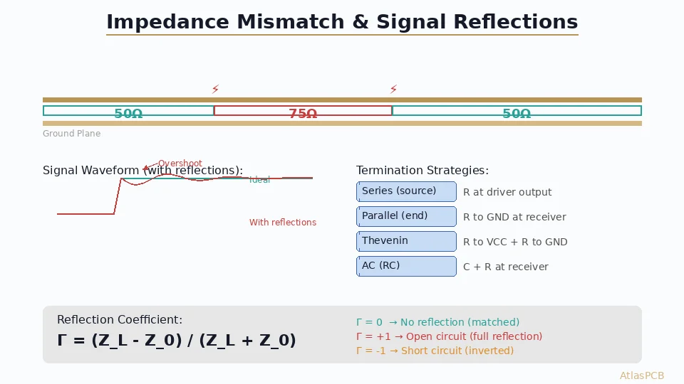
Reflections and Impedance Discontinuities
Every impedance discontinuity along the signal path creates a reflection. In a backplane, the most common sources include:
- Via transitions between routing layers
- Connector pin fields
- Trace width changes at breakout regions
- Reference plane gaps or splits
Even a 5% impedance deviation at a single via can produce reflections that degrade the eye diagram at 25 Gbps. This is why [impedance control]/blog/pcb-impedance-control/) in backplane manufacturing requires tighter tolerances than standard PCBs — typically ±5% to ±7% rather than the ±10% acceptable for lower-speed designs.
![Backplane signal integrity loss budget diagram showing dielectric, conductor, and connector loss contributions]/blog/pcb-backplane-design-high-speed/)
Material Selection for High-Speed Backplanes
Laminate Classification by Loss Performance
PCB laminates are broadly categorized by their loss performance at high frequencies. For backplane applications, understanding these categories is essential:
| Category | Df Range (at 10 GHz) | Typical Applications |
|---|---|---|
| Standard FR-4 | 0.018–0.022 | Backplanes ≤ 3 Gbps |
| Mid-loss FR-4 | 0.010–0.015 | Backplanes at 5–10 Gbps |
| Low-loss | 0.005–0.008 | Backplanes at 10–16 Gbps |
| Very low-loss | 0.003–0.005 | Backplanes at 25–56 Gbps |
| Ultra low-loss | <0.003 | Backplanes at 56+ Gbps (PAM4) |
For modern backplane designs targeting 25 Gbps and above, very low-loss materials are essentially mandatory. The cost premium over standard FR-4 is significant — often 3–5× for raw laminate — but the alternative is a non-functional design.
For a deeper comparison of high-speed materials and their electrical properties, see our [Dk/Df material comparison guide]/blog/pcb-high-speed-material-dk-df-comparison/).
Copper Foil Selection
Copper surface roughness directly impacts conductor loss at high frequencies due to the skin effect. As frequency increases, current flows in an increasingly thin layer at the conductor surface, and rough surfaces increase the effective path length.
Three copper foil profiles are commonly available:
- Standard (STD) — Rz ≈ 10 µm. Adequate for backplanes below 5 Gbps.
- Reverse-treated (RTF) — Rz ≈ 5 µm. Suitable for 10–16 Gbps backplanes.
- Very low-profile (VLP) — Rz ≈ 3 µm. Required for 25 Gbps and above.
- Hyper very low-profile (HVLP) — Rz ≤ 2 µm. Preferred for 56 Gbps PAM4.
The trade-off with smoother foils is reduced adhesion to the laminate. VLP and HVLP foils require oxide alternative or silane-based adhesion promotion treatments to maintain reliable bonding during lamination and throughout the product lifetime.
Glass Weave Effects
The woven glass reinforcement in FR-4 and most high-speed laminates creates a non-uniform dielectric environment. The Dk of glass fiber (approximately 6.2) differs significantly from the Dk of resin (approximately 3.0), creating periodic Dk variations across the board surface.
For backplane differential pairs, this “fiber weave effect” can cause intra-pair skew when one trace of a pair sits over glass bundles while the other sits over resin-rich areas. At 25 Gbps, just 5 ps of intra-pair skew can measurably degrade the eye diagram.
Mitigation strategies include:
- Routing at angles to the weave pattern (typically 5–11° off-axis)
- Using spread-glass or flat-glass fabric styles (e.g., 1078 or 1035 instead of 7628)
- NE-glass variants that have a Dk closer to the resin, reducing the contrast
Stackup Architecture for Backplane Performance
Layer Count and Signal Layer Placement
High-speed backplanes typically require 20–40 or more layers, depending on connector density and channel count. The stackup architecture must balance several competing requirements:
- Signal layers must be adjacent to continuous ground reference planes
- Power distribution requires dedicated plane pairs for each voltage rail
- Mechanical symmetry prevents warpage during lamination and reflow
- Manufacturing capability limits total thickness and minimum dielectric spacing
A common approach for a 24-layer backplane:
- 8–10 signal layers (stripline configuration)
- 10–12 ground/power planes
- 2 outer layers for component placement and low-speed signals
Every high-speed signal layer should be referenced to a solid ground plane on at least one adjacent layer. Dual-referenced stripline (ground planes on both sides) provides the best shielding and crosstalk isolation.
For detailed guidance on building an effective stackup, refer to our [multilayer PCB stackup design guide]/blog/multilayer-pcb-stackup-design-guide/).
Dielectric Thickness and Impedance Targets
Most high-speed backplane standards specify either 85 Ω or 100 Ω differential impedance. Achieving these targets with tight tolerance requires precise control of:
- Dielectric thickness between the signal layer and reference plane
- Trace width and spacing within differential pairs
- Dk of the laminate at the operating frequency
For 85 Ω edge-coupled differential stripline with a typical very low-loss laminate (Dk ≈ 3.6):
- Dielectric thickness: 5–6 mil per side
- Trace width: 4–5 mil
- Pair spacing (edge-to-edge): 6–8 mil
These dimensions demand manufacturing capability at the HDI level, even though the backplane itself may not use HDI features like microvias.
Back-Drilling for Via Stub Removal
Via stubs are one of the most significant signal integrity problems in thick backplane PCBs. When a signal transitions from one internal layer to another through a through-hole via, the unused portion of the via barrel acts as a resonant stub that creates a notch in the frequency response.
For a 250-mil-thick backplane with a signal transition at layer 4, the remaining via stub extends approximately 200 mil — creating a quarter-wave resonance near 7.5 GHz. This completely destroys signal quality at 25 Gbps.
[Back-drilling]/blog/pcb-back-drill/) removes the unused stub, typically leaving only 6–10 mil of residual stub. For backplanes at 25 Gbps and above, back-drilling is not optional — it is a fundamental design requirement.
Key back-drilling specifications:
- Stub length target: ≤ 10 mil residual
- Positional accuracy: ±3 mil registration to the drilled hole
- Drill depth tolerance: ±4 mil from target depth
- Minimum remaining copper: 8 mil from the signal connection pad to the drill tip
Differential Pair Routing Strategies
Breakout from High-Density Connectors
The connector breakout region is often the most challenging area of a backplane layout. Modern high-speed connectors (press-fit or SMT) use pin pitches of 1.0–2.0 mm, requiring the router to escape dozens or hundreds of differential pairs through a congested pin field.
Best practices for connector breakout:
- Route inner rows first — inner pin rows need the most via transitions to escape, so allocate deeper signal layers for inner rows
- Maintain differential pair coupling through the entire breakout — never allow a pair to become uncoupled, even briefly
- Use ground vias liberally between signal via pairs to provide shielding and maintain reference plane integrity
- Match via structures within each pair — both traces should use identical via types and layer transitions
For additional [differential pair routing]/blog/differential-pair-routing-pcb/) techniques, our dedicated guide covers coupling modes, length matching, and return path management.
Length Matching and Skew Budget
Backplane designs must manage skew at two levels:
- Intra-pair skew (between the P and N traces of a single pair): typically ≤ 5 mil length difference for 25 Gbps, equivalent to approximately 1 ps of skew
- Inter-pair skew (between pairs within a group): defined by the protocol. PCIe Gen 4 allows up to 20 ns between lanes in a link.
Intra-pair skew is more critical for signal integrity because it directly converts differential signal energy into common-mode noise. The primary causes are:
- Asymmetric routing around obstacles
- Different via pad sizes within a pair
- Glass weave effects (discussed above)
- Non-symmetric reference plane features
Use serpentine (trombone) tuning to match lengths, but keep serpentine segments short and tight. The accordion pattern should have a maximum amplitude of 3× the trace width and a pitch of at least 5× the trace width to avoid self-coupling.
Reference Plane Management
Every high-speed signal on a backplane needs a continuous, unbroken reference plane. When a signal must change layers, the reference plane often changes too — and the return current must be able to follow.
Rules for reference plane management in backplanes:
- Place stitching vias adjacent to every signal via pair, connecting the old reference plane to the new one
- Never route high-speed signals over splits or gaps in the reference plane
- Dedicate ground planes as references rather than power planes, since power planes often have splits for different voltage domains
- Add ground via fences along the edges of dense routing channels to contain fields and reduce crosstalk
For more on grounding strategy, see our guide on [PCB grounding techniques]/blog/pcb-grounding-techniques/).
Power Distribution for Backplane Systems
PDN Design Considerations
While signal integrity gets most of the attention in backplane design, the power distribution network (PDN) is equally critical. A noisy or high-impedance PDN degrades signal quality by modulating the reference voltages that high-speed signals are measured against.
Backplane PDN design must address:
- Bulk decoupling at each connector site to supply transient current demands from daughter cards
- Plane pair impedance that remains below the target impedance across the frequency range of interest
- Via and trace current capacity for the total current drawn by all daughter cards
- Voltage drop across the backplane, which can be significant given the long distances and high currents involved
For a comprehensive treatment of power distribution, see our [power plane design and PDN analysis guide]/blog/pcb-power-plane-design-split-planes-pdn-analysis/).
Decoupling Strategy
Place bulk decoupling capacitors (10–100 µF) at each daughter card connector location. Add mid-frequency capacitors (100 nF–1 µF) distributed across the backplane surface between connectors. The plane pair capacitance handles high-frequency decoupling above approximately 500 MHz.
Manufacturing Considerations
Registration and Drill Accuracy
Backplane PCBs push manufacturing registration limits due to their size and layer count. A 20×16-inch, 30-layer backplane requires:
- Layer-to-layer registration: ±3 mil or better
- Drill registration: ±2 mil to achieve reliable annular rings
- Back-drill registration: ±3 mil to the original through-hole
These tolerances are achievable but require experienced multilayer PCB manufacturers with appropriate equipment and process controls.
Impedance Testing
Every production backplane should undergo impedance verification via TDR (time-domain reflectometry) testing on dedicated coupon structures. The test coupons must replicate the actual stackup, trace geometries, and via structures used in the production design.
Specify TDR testing to the appropriate standard (IPC-TM-650, Method 2.5.5.7) with tolerance limits that match your design requirements. For 25 Gbps backplanes, request ±5% impedance tolerance with 100% coupon testing per panel.
For broader [PCB testing methodologies]/blog/pcb-testing-methods/), our testing guide covers additional electrical and reliability tests relevant to backplane production.
Design Verification and Simulation
Pre-Layout Simulation
Before routing begins, simulate the target channel to establish feasibility:
- Define the channel — connector models (S-parameter), via models, trace lengths, and material properties
- Run insertion loss analysis — verify the channel meets the loss budget at the Nyquist frequency
- Simulate eye diagrams — apply transmitter pre-emphasis and receiver equalization models
- Check compliance — compare simulation results against the target standard’s channel specification
Post-Layout Verification
After routing, extract the actual geometries and re-simulate:
- 3D electromagnetic simulation of critical via transitions and connector breakout regions
- Full-channel S-parameter extraction from transmitter pad to receiver pad
- Crosstalk analysis using multi-aggressor simulation with realistic switching patterns
- Power integrity simulation to verify PDN impedance and voltage drop
Backplane Design Checklist
Before releasing a high-speed backplane design for manufacturing, verify:
- All differential pairs meet impedance targets with ≤ ±7% tolerance
- Intra-pair skew is within protocol requirements
- Via stubs are back-drilled with ≤ 10 mil residual
- Reference planes are continuous beneath all high-speed routes
- Ground stitching vias are placed at every layer transition
- Crosstalk spacing rules are met throughout
- PDN impedance meets target across the frequency range
- [DFM requirements]/blog/pcb-dfm-checklist/) are satisfied for the target manufacturer
- Insertion loss simulations confirm compliance at Nyquist frequency
- Connector footprints match vendor specifications
Conclusion
High-speed backplane PCB design sits at the intersection of electromagnetic engineering, materials science, and precision manufacturing. Success requires a systematic approach: start with the channel loss budget, select materials and stackup to meet that budget, route with disciplined attention to impedance and crosstalk, and verify through simulation before committing to fabrication.
The difference between a backplane that works at 25 Gbps and one that does not is often found in the details — a few extra mils of via stub, a glass weave interaction that adds skew, or a reference plane gap that creates a resonance. Partnering with a manufacturer that understands these subtleties is essential.
Ready to build your next high-speed backplane?
Upload your Gerbers for a free engineering review — our team will analyze your stackup, impedance targets, and signal integrity requirements. Get a quote today →
Further Reading
- [PCB Design for GaN and SiC Power Devices: Thermal Management, Layout Rules, and Material Selection]/blog/pcb-design-gan-sic-power-devices-thermal-layout/)
- [PCB Panelization and Array Design: V-Score vs Tab Routing, DFM Rules, and Cost Optimization]/blog/pcb-panelization-v-score-tab-routing-dfm-cost-optimization/)
- [mmWave PCB Material Selection: Rogers vs Megtron vs LCP for 5G and 6G Applications]/blog/mmwave-pcb-material-selection-rogers-megtron-lcp-5g-6g/)
- [Rogers PCB Fabrication: Material Sourcing, Lead Times & Quality Control]/blog/rogers-pcb-fabrication/)
- [PCB Rigid-Flex Bend Zone Reliability: Design Rules, Material Selection & Lifecycle Testing]/blog/pcb-rigid-flex-bend-zone-reliability/)
- Rigid PCB Manufacturing
About AtlasPCB — We specialize in complex PCB manufacturing for HDI, RF, and high-reliability applications. Explore our impedance-controlled PCB manufacturing . Every order includes free engineering review. Get your quote.
Reviewed by AtlasPCB Engineering Team — IPC-certified manufacturing specialists with 15+ years of production experience in HDI, RF, and high-reliability PCB fabrication. Content based on factory floor data and real customer design reviews.
- backplane
- high-speed
- signal-integrity
- impedance
- differential-pairs