· AtlasPCB Engineering · Engineering · 11 min read
PCB Copper Pour and Ground Plane Design: Best Practices for Signal Integrity
Master copper pour and ground plane design for EMI shielding and signal integrity. Learn ground plane partitioning, stitching vias, clearance rules, and thermal relief strategies.
Introduction: The Foundation of Every Good PCB Design
If you were to strip away everything in a PCB design except the ground planes, you would still see the skeleton of the entire system’s electromagnetic behavior. Ground planes and copper pours are not just “fill” — they are the reference surfaces against which every signal propagates, every return current flows, and every EMI boundary is defined.
Despite their fundamental importance, copper pours and ground planes are frequently treated as an afterthought: “just flood everything with GND and move on.” This approach works for low-frequency, non-critical designs. For anything involving controlled impedance, high-speed digital signals, sensitive analog circuits, or EMC compliance, ground plane design requires deliberate engineering.
This guide covers the principles, rules, and practical techniques for designing copper pours and ground planes that support signal integrity, minimize EMI, and survive the manufacturing process. The content applies to designs from 2-layer boards through complex 20+ layer stackups.
Ground Plane Fundamentals
Why Ground Planes Matter
A ground plane serves three critical functions:
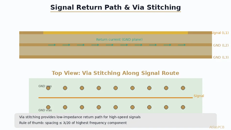
Low-impedance return current path: Every signal requires a return path. A continuous ground plane directly beneath a signal trace provides the lowest-inductance return path, with current naturally concentrating in a strip directly below the trace (within approximately 3× the trace-to-plane separation on either side).
Electromagnetic shielding: A continuous copper plane blocks electric field coupling between layers and contains electromagnetic radiation within the board structure. A solid ground plane provides >40 dB of isolation between the layers it separates.
Reference for controlled impedance: Microstrip and stripline impedances are defined by the trace’s relationship to the nearest reference plane. An incomplete or disrupted reference plane creates unpredictable impedance variations.
For a deep dive into impedance design, see our [controlled impedance PCB guide]/blog/controlled-impedance-pcb/).
Return Current Behavior
Understanding return current is essential for ground plane design:
- At DC and low frequencies (<1 kHz): Return current follows the path of least resistance, spreading across the entire plane.
- At high frequencies (>100 kHz): Return current follows the path of least inductance, concentrating directly beneath the signal trace in a strip approximately 3× the dielectric thickness on each side.
- At the transition zone (1 kHz – 100 kHz): Return current gradually transitions from resistive to inductive path selection.
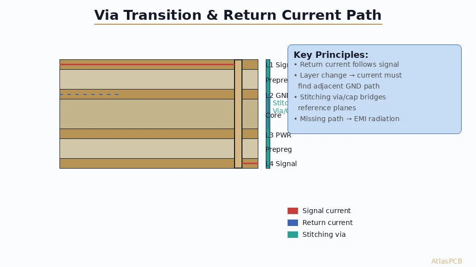
This frequency-dependent behavior has a critical design implication: any slot, split, or void in the ground plane that interrupts the return current path beneath a signal trace forces the return current to detour around the obstruction, creating a loop antenna that radiates EMI and degrades signal quality.
Copper Pour Design Rules
Solid Fill vs. Hatched Fill
The debate between solid and hatched copper fill has a clear winner for signal integrity:
Solid fill advantages:
- Lowest impedance return path
- Best EMI shielding effectiveness
- Predictable impedance control
- Better thermal conduction
- Uniform current distribution
Hatched fill limitations:
- Each opening acts as a slot antenna
- Unpredictable impedance at high frequencies
- Reduced shielding effectiveness (10-20 dB less than solid)
- Creates resonant structures at specific frequencies
When hatched fill is appropriate:
- Flex and rigid-flex circuits where solid copper would restrict bending
- Non-critical areas far from sensitive signals
- Specific thermal management scenarios requiring controlled heat flow
Design rule: Use solid fill for all ground planes and power planes. If copper balance is a concern, work with your fabricator to adjust process parameters rather than compromising electromagnetic performance with hatched fill.
Copper Pour Clearance Rules
The clearance between a copper pour and adjacent features determines both electrical isolation and electromagnetic coupling:
| Feature | Minimum Clearance (Standard) | Minimum Clearance (High-Speed) |
|---|---|---|
| Signal traces | 0.25 mm (10 mil) | 0.30 mm (12 mil) or 2× dielectric thickness |
| Component pads | 0.25 mm (10 mil) | 0.30 mm (12 mil) |
| Other copper pours | 0.25 mm (10 mil) | 0.50 mm (20 mil) |
| Board edge | 0.50 mm (20 mil) | 0.50 mm (20 mil) |
| Via pads (same net) | 0 (direct connect) | 0 (direct connect) |
| Via pads (different net) | 0.25 mm (10 mil) | 0.30 mm (12 mil) |
High-voltage considerations: For voltages exceeding 50V, consult IPC-2221 Table 6-1 for minimum clearance values. Internal layer clearances differ from external layer values due to the higher dielectric withstand voltage of laminate compared to air.
Orphan Copper (Isolated Copper Islands)
Copper islands that are not connected to any net (orphan copper) are a manufacturing and reliability concern:
- Acid traps: Small isolated copper areas can trap etchant, causing incomplete etching
- Antenna effects: Ungrounded copper can act as a receiving antenna, coupling noise into nearby traces
- Solder bridging: On outer layers, isolated copper near pads can cause solder bridging during assembly
Design rule: Set your EDA tool to automatically remove copper islands below a minimum size (typically 0.5 mm² for inner layers, 1.0 mm² for outer layers). Manually verify that remaining islands serve a purpose.
Copper Balance
Uneven copper distribution between the top and bottom of a PCB causes bow and twist during lamination and soldering:
- IPC-6012 limit: Bow and twist ≤0.75% for surface mount assemblies
- Target: <10% copper area difference between opposing layers in any board quadrant
- Methods to achieve balance:
- Add copper fill (thieving) to sparse layers
- Use ground/power pours on all layers
- Add non-functional copper patterns in border areas
- Coordinate with your fabricator on panel-level balancing
Your fabricator can advise on copper balance requirements for your specific stackup. See our [PCB manufacturing process guide]/blog/pcb-manufacturing-process-15-steps/) for details on how copper distribution affects lamination.
Ground Plane Design Strategies
Single Ground Plane (2-4 Layer Boards)
For 2-layer boards, the ground plane is typically on Layer 2 (bottom):
- Route all critical signals on Layer 1 (top) with the ground plane on Layer 2
- Use short traces on Layer 2 only for non-critical connections
- Every trace on Layer 1 that crosses a trace on Layer 2 creates a potential return path disruption — minimize these crossings
- Place decoupling capacitors as close as possible to IC power pins
For 4-layer boards, the standard stackup is:
| Layer | Function |
|---|---|
| L1 | Signal + components |
| L2 | Ground plane (continuous) |
| L3 | Power plane |
| L4 | Signal + components |
This arrangement places a ground plane immediately adjacent to both signal layers, providing excellent return current paths and impedance control. For stackup optimization, use our [PCB stackup calculator]/blog/pcb-stackup-calculator/).
Multiple Ground Planes (6+ Layer Boards)
In boards with 6 or more layers, multiple ground planes offer enhanced isolation:
8-layer example:
| Layer | Function |
|---|---|
| L1 | Signal (high-speed) |
| L2 | Ground |
| L3 | Signal (general) |
| L4 | Power |
| L5 | Ground |
| L6 | Signal (general) |
| L7 | Ground |
| L8 | Signal (high-speed) |
Key principles:
- Every signal layer has an adjacent ground plane for return current
- Ground planes on L2 and L7 provide shielding for outer-layer high-speed signals
- The L5 ground plane isolates the upper and lower halves of the board
- All ground planes must be connected with stitching vias
Ground Plane Splits and Partitioning
Ground plane splits are sometimes used to isolate analog and digital sections. This is one of the most misunderstood topics in PCB design:
When ground splits are appropriate:
- Mixed-signal designs with very high-resolution ADCs/DACs (≥18-bit)
- Designs with high-current switching noise (>10A transients) that would corrupt sensitive analog circuits
- RF sections that require a dedicated, ultra-clean ground reference
When ground splits cause more harm than good:
- Low-to-moderate resolution mixed-signal circuits (<16-bit)
- Designs where digital signals must route across the split boundary
- Boards where the split creates large return current loops
Best practice for mixed-signal design:
- Use a single, continuous ground plane
- Partition the component placement so analog and digital components occupy separate regions
- Route digital return currents through one area and analog return currents through another — the current naturally separates on a continuous plane
- Connect ADC/DAC AGND and DGND pins to the single ground plane directly at the IC
This approach provides the low-impedance grounding needed for both domains without creating the return path disruptions that splits cause. For more on grounding strategies, see our [PCB grounding techniques guide]/blog/pcb-grounding-techniques/).
Stitching Vias: Connecting Ground Planes
Purpose and Placement
Stitching vias connect multiple ground planes through the board, ensuring they remain at the same potential at all frequencies:
- Edge stitching: Vias along board edges create a Faraday cage effect, containing EMI within the board
- Area stitching: Vias distributed across the ground plane area ensure uniform potential
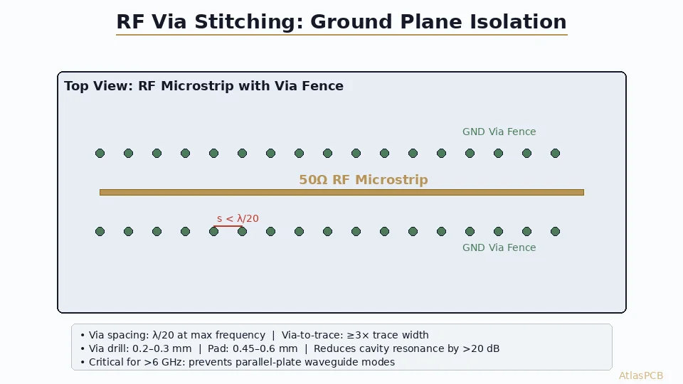
- Via fence: Dense via arrays around sensitive areas (oscillators, RF sections) for isolation
Spacing Rules
The maximum effective spacing between stitching vias depends on the highest frequency of interest:
| Frequency | Maximum Via Spacing (λ/20) | Recommended Spacing |
|---|---|---|
| 100 MHz | 150 mm | 100 mm |
| 500 MHz | 30 mm | 20 mm |
| 1 GHz | 15 mm | 10 mm |
| 3 GHz | 5 mm | 3 mm |
| 5 GHz | 3 mm | 2 mm |
| 10 GHz | 1.5 mm | 1 mm |
Design rule: Calculate the maximum spacing based on the highest frequency harmonic present on your board (typically the 5th harmonic of your fastest clock), then use λ/20 as the maximum pitch.
Via Fence Design
For critical isolation, a via fence requires:
- Via-to-via pitch ≤ λ/20 of the highest frequency
- Vias connecting all ground planes in the stackup
- Continuous copper on both sides of the fence (no gaps in ground planes at the fence location)
- Via drill size: 0.3-0.5 mm is typical; smaller vias provide denser packing
EMI Considerations in Ground Plane Design
Proper ground plane design is one of the most effective EMI reduction techniques, often more impactful than adding shields or filters after the fact. For comprehensive EMI design strategies, see our [EMC/EMI PCB design guide]/blog/emc-emi-pcb-design/).
Common EMI-Generating Ground Plane Mistakes
- Slots in ground plane under high-speed traces: A slot forces return current to flow around it, creating a loop antenna proportional to the slot length × detour distance
- Split plane with signals crossing the split: Same effect as a slot — return current cannot follow the signal, creating radiation
- Missing stitching vias at connector regions: Connectors are primary EMI egress points; dense ground vias near connectors are essential
- Ground pour connected at only one point: A ground pour connected by a single thin trace becomes a resonant patch antenna at frequencies where its dimensions approach λ/4
20H Rule
The 20H rule states that the ground plane should extend at least 20× the dielectric thickness (H) beyond the edge of the power plane on all sides. This “fringing field containment” reduces edge-radiated EMI from the power-ground cavity:
- For H = 0.1 mm: Extend ground by 2.0 mm beyond power plane edge
- This rule applies to power plane boundaries, not board edges
- Effectiveness: ~10 dB reduction in edge radiation at the cavity resonance frequencies
Thermal Considerations
Copper Pour for Heat Spreading
Copper’s thermal conductivity (385 W/m·K) makes it an excellent heat spreader. Copper pours on multiple layers, connected with thermal vias, can significantly reduce component temperatures:
- Thermal via array: 0.3 mm drill, 0.6 mm pitch, under thermal pads
- Copper pour area: Extend at least 5 mm beyond the heat source in all directions
- Multi-layer connection: Connect the thermal pour on all available layers with vias
For detailed thermal management techniques, see our [PCB thermal management guide]/blog/pcb-thermal-management/).
Thermal Relief Pads in Ground Pours
Thermal relief pads balance solderability with electrical/thermal performance:
| Connection Type | Thermal Resistance | Solderability | Use When |
|---|---|---|---|
| Direct connect | Lowest | Poor (hand solder) | High-current paths, thermal management |
| 4-spoke thermal relief | Low-moderate | Good | Standard SMD and through-hole |
| 2-spoke thermal relief | Moderate | Excellent | Large ground pins, hand-solder critical |
Design rule for high-current ground connections: Use direct connection for ground pins carrying >1A or where thermal performance is critical. Use thermal relief for standard signal and low-current ground connections.
DFM Considerations for Copper Pour
Acid Traps
Acute angles (<90°) in copper features trap etchant and cause over-etching. In copper pours, acid traps form where pour edges create acute angles with traces or pads:
- Set minimum copper pour acute angle to 90°
- Use rounded (chamfered) pour corners where possible
- Maintain adequate clearance to prevent narrow copper slivers
Solder Mask Dam
On outer layers, copper pour near SMD pads requires adequate solder mask dams to prevent solder bridging:
- Minimum solder mask dam width: 0.075 mm (3 mil) for standard; 0.10 mm (4 mil) recommended
- Copper pour to pad clearance: Must account for solder mask registration tolerance (typically ±0.05 mm)
- Solder mask defined vs. copper defined pads: Copper pour proximity changes the effective pad definition
Review the complete [DFM checklist]/blog/pcb-dfm-checklist/) for additional copper pour manufacturing guidelines.
Copper Balancing (Thieving)
Fabricators add non-functional copper patterns (thieving) in sparse areas to balance copper density. This affects:
- Etch uniformity: Even copper density ensures consistent trace width control
- Lamination pressure distribution: Balanced copper prevents resin starvation and thickness variation
- Bow and twist: Symmetric copper distribution minimizes warpage
Best practice: Add ground pour to all layers, filling unused areas with copper connected to the ground net. This simultaneously provides EMI shielding and copper balance.
Practical Ground Plane Design Checklist
Use this checklist when reviewing your ground plane design:
- Every signal layer has an adjacent reference plane (ground or power)
- No signal traces cross ground plane splits or slots
- Stitching vias connect all ground planes at ≤λ/20 spacing
- Board edge has stitching vias at ≤λ/20 spacing
- Critical signals (clocks, high-speed data) have uninterrupted ground plane beneath their entire route
- Connector ground pins have nearby stitching vias
- No orphan copper islands
- Copper pour clearance set appropriately for voltage and impedance requirements
- Thermal relief pads used only where needed — direct connection for high-current paths
- Ground plane extends ≥20H beyond power plane edges (20H rule)
- No acute angles (<90°) in copper pour geometry
- Copper distribution balanced between top and bottom layer groups
Conclusion
Copper pour and ground plane design is where electrical engineering meets electromagnetic physics. The decisions you make about ground plane continuity, stitching via placement, split strategies, and pour clearances will determine whether your board meets EMC requirements on the first spin or requires multiple costly redesigns.
The overarching principle is simple: keep ground planes continuous and uninterrupted beneath signal traces. Every slot, split, and void is a potential EMI source and signal integrity degradation point. When you must partition power domains, do so with power planes while keeping ground continuous.
At Atlas PCB, our engineering team reviews stackup designs and ground plane strategies as part of every DFM review. Whether you are designing a 4-layer IoT module or a 24-layer backplane, we can help optimize your copper pour strategy for both manufacturability and performance.
Atlas PCB specializes in controlled impedance PCBs with optimized stackup designs and comprehensive DFM review. Contact us for engineering support and a free DFM review on your next project.
Further Reading
- [HDI PCB Design for 5G Antenna Integration: Signal Integrity Challenges in Millimeter-Wave Applications]/blog/hdi-5g-antenna-integration-pcb-design/)
- [PCB Impedance Matching and Differential Pair Design: Spacing, Length Matching, and Layout]/blog/pcb-impedance-matching-differential-pairs/)
- [Controlled Impedance PCB Stackup Design: Rules, Calculations, and Manufacturing Tolerances for High-Speed Designs]/blog/controlled-impedance-pcb-stackup-design-rules/)
- [PCB Stackup Calculator: Layer Count, Material & Impedance Planning]/blog/pcb-stackup-calculator/)
- [PCB Dielectric Constant (Dk) Measurement: Methods, Accuracy & Impact on Impedance Control]/blog/pcb-dielectric-constant-dk-measurement/)
- Rigid PCB Manufacturing
About AtlasPCB — We specialize in complex PCB manufacturing for HDI, RF, and high-reliability applications. Explore our impedance-controlled PCB manufacturing . Every order includes free engineering review. Get your quote.
Reviewed by AtlasPCB Engineering Team — IPC-certified manufacturing specialists with 15+ years of production experience in HDI, RF, and high-reliability PCB fabrication. Content based on factory floor data and real customer design reviews.
- copper-pour
- ground-plane
- signal-integrity
- emi-shielding