· AtlasPCB Engineering · Engineering · 9 min read
Differential Impedance Control for PCIe Gen5 and DDR5: Microstrip vs. Stripline Routing Strategies
Master differential impedance control for PCIe Gen5 (32 GT/s) and DDR5 (6400+ MT/s) interfaces. Compare microstrip and stripline routing, understand coupling effects, design stackups for 85Ω and 100Ω differential impedance, and learn practical tolerance budgeting for high-speed SerDes signaling.
Introduction: The Impedance Challenge at 32 GT/s and Beyond
Modern high-speed interfaces operate at data rates that push PCB transmission line design to its limits. PCIe Gen5 at 32 GT/s uses NRZ signaling with a fundamental frequency of 16 GHz — meaning the fifth harmonic extends to 80 GHz and even the third harmonic at 48 GHz carries significant signal energy. DDR5 at 6400 MT/s creates a single-data-rate clock of 3.2 GHz, with signal rise times under 50 ps requiring bandwidth preservation beyond 14 GHz.
At these frequencies, every aspect of the differential pair geometry matters: trace width tolerance (±0.5 mil impacts impedance by ±2Ω), dielectric thickness variation (±0.5 mil changes impedance by ±3Ω), copper roughness profile (Rz affects loss by 15–30% at 16 GHz), and glass weave orientation relative to trace routing (±2Ω impedance variation from fiber weave effect).
This article provides the engineering framework for designing differential impedance structures that meet PCIe Gen5 and DDR5 specifications, comparing microstrip and stripline approaches with quantified trade-offs for each topology.
Fundamental Differential Pair Physics
What Creates Differential Impedance
Differential impedance (Z_diff) describes the impedance seen by a differential signal — the voltage difference between two conductors carrying complementary signals. For a loosely-coupled pair:
Z_diff = 2 × Z_odd = 2 × Z0 × (1 - k_coupling)
Where Z0 is the isolated single-ended impedance and k_coupling is the mutual coupling coefficient (0 for no coupling, approaching 1 for tight coupling).
For typical PCB differential pairs:
- Loosely coupled (space > 3× width): Z_diff ≈ 2 × Z0
- Tightly coupled (space = width): Z_diff ≈ 1.6–1.8 × Z0
- Edge-coupled stripline: k typically 0.05–0.20
- Edge-coupled microstrip: k typically 0.03–0.15
Coupling Trade-offs
Tight coupling (space ≤ trace width):
- Lower differential impedance for given trace width
- Better common-mode noise rejection (CMRR)
- Tighter routing density
- More susceptible to intra-pair skew from manufacturing
- Higher crosstalk to adjacent pairs
Loose coupling (space > 2× trace width):
- Differential impedance approaches 2× single-ended
- Less sensitive to spacing tolerance
- More routing flexibility
- Worse CMRR
- Easier to achieve impedance target with standard processes
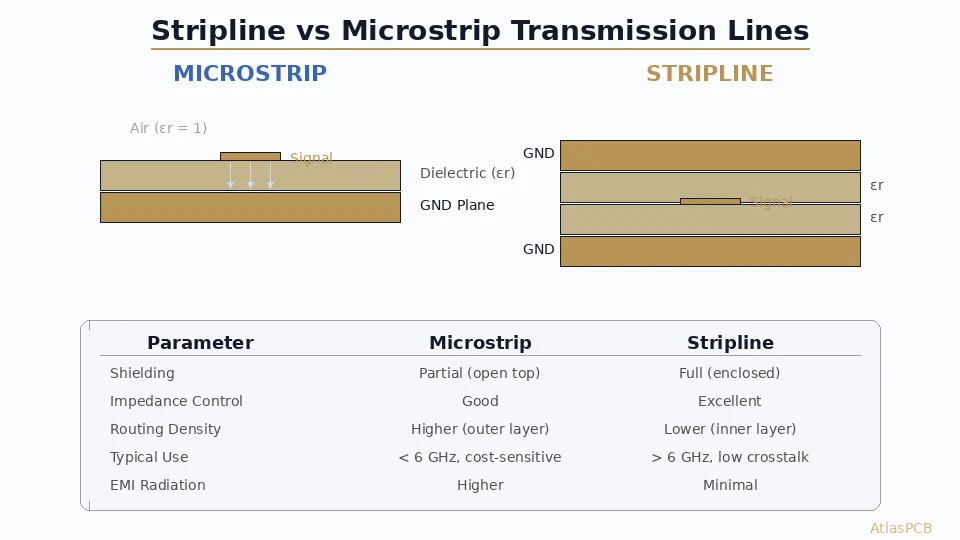
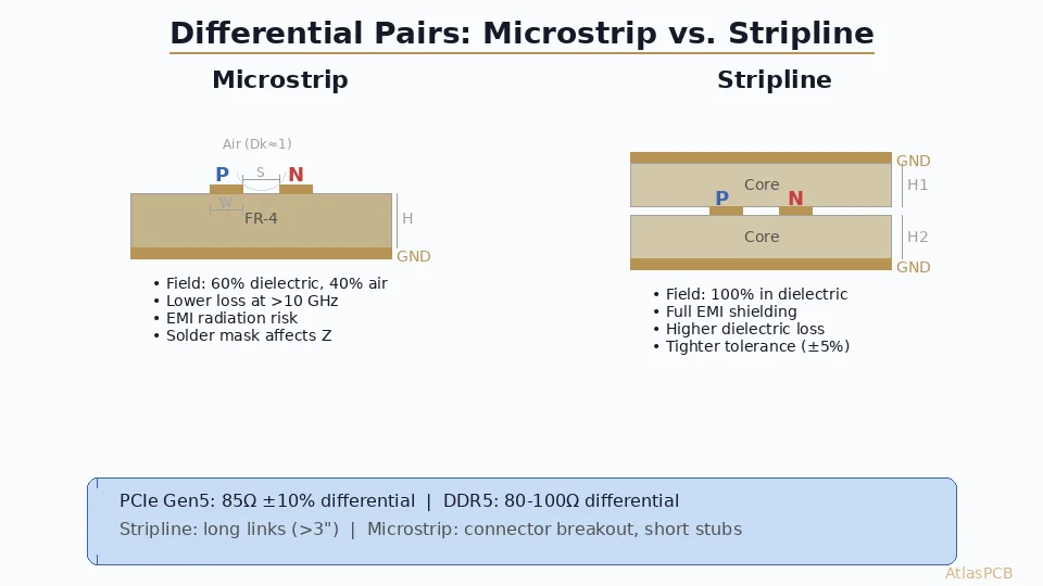
Microstrip Differential Pairs
Geometry and Field Distribution
Microstrip differential pairs sit on the outer PCB layer with a single ground/power reference plane below. The electromagnetic fields travel partially in the dielectric substrate and partially in air (or solder mask), creating an effective dielectric constant (Dk_eff) that is lower than the bulk substrate Dk.
Key parameters:
- W: Trace width (typical 3.5–5.0 mil for 85Ω diff on standard materials)
- S: Gap between traces (typical 4.0–8.0 mil)
- H: Dielectric height to reference plane (typical 3.0–5.0 mil)
- T: Copper thickness (0.5–2.0 oz, affects impedance by ±1–3Ω)
- Dk_eff: Effective dielectric constant (~0.6 × Dk_bulk + 0.4 × Dk_air for surface microstrip)
Advantages for High-Speed Design
- Lower dielectric loss: ~40% of field energy travels in air/mask (Df ≈ 0), reducing total loss
- Accessible for probing: Test points and measurement coupons on outer layer
- Simpler stackup: Only one reference plane required per pair
- Better impedance predictability at high frequency: Air portion has frequency-independent Dk
- Lower phase constant variation: Less dispersive than stripline at > 10 GHz
Disadvantages
- EMI radiation: Fields extend into air; differential pairs radiate at common-mode conversion points
- Environmental sensitivity: Humidity, conformal coating, and solder mask affect impedance
- Etch factor sensitivity: Trapezoidal cross-section from etching changes effective width
- Coupling variation: Solder mask buildup between traces changes coupling
Design Example: 85Ω Differential Microstrip for PCIe Gen5
Target: 85Ω ±8% differential, Megtron 6 (Dk = 3.4, Df = 0.002 at 12 GHz)
Stackup:
- Signal layer L1 (0.5 oz copper, 18 μm)
- Prepreg: 3.5 mil (89 μm) Megtron 6, Dk = 3.4
- Reference GND plane L2
Calculated geometry (2D field solver — Polar Si9000):
- Trace width: 3.8 mil (97 μm)
- Spacing: 5.0 mil (127 μm)
- Result: Z_diff = 85.2Ω, Z_odd = 42.6Ω
- Coupling coefficient: k = 0.08 (loosely coupled)
Manufacturing tolerance budget:
- Width ±0.3 mil → ±2.1Ω
- Height ±0.3 mil → ±2.5Ω
- Dk ±0.05 → ±1.0Ω
- RSS total: ±3.4Ω (±4.0%) — well within ±8% target
Stripline Differential Pairs
Geometry and Field Distribution
Stripline differential pairs are embedded between two reference planes (GND-signal-GND or GND-signal-PWR). All electromagnetic fields are contained within the dielectric, creating a fully-shielded transmission line.
Key parameters:
- W: Trace width (typically 3.0–4.5 mil for 100Ω diff)
- S: Gap between traces
- H1: Distance to upper reference plane
- H2: Distance to lower reference plane (symmetric: H1 = H2)
- Dk: Full bulk dielectric constant (no air fraction)
Advantages
- Complete EMI shielding: No radiation; ideal for sensitive analog/RF nearby
- Stable impedance: No environmental sensitivity (sealed in dielectric)
- Tighter tolerance: Lamination presses control dielectric thickness ±0.3 mil
- Symmetric environment: Both traces see identical field distribution (better CMRR)
- No solder mask compensation needed
Disadvantages
- Higher dielectric loss: 100% of field in lossy dielectric material
- Thicker stackup: Two reference planes per signal layer add cost/thickness
- Difficult probing: Cannot access embedded traces for measurement
- Via transitions required: Signals must via to/from components on outer layers
- Higher Dk: Full Dk (vs. effective Dk for microstrip) means narrower traces for same impedance
Design Example: 85Ω Differential Stripline for PCIe Gen5
Target: 85Ω ±7% differential, Megtron 6 (Dk = 3.6 at 10 GHz, core material)
Stackup (symmetric):
- Reference GND plane above
- Core: 4.0 mil (102 μm) Megtron 6, Dk = 3.6
- Signal layer (0.5 oz copper)
- Core: 4.0 mil symmetric below
- Reference GND plane below
Calculated geometry:
- Trace width: 3.2 mil (81 μm)
- Spacing: 6.0 mil (152 μm)
- Result: Z_diff = 85.4Ω, Z_odd = 42.7Ω
- Coupling coefficient: k = 0.06
Manufacturing tolerance budget:
- Width ±0.3 mil → ±2.4Ω
- Height ±0.3 mil → ±1.8Ω (two planes averaging)
- Dk ±0.05 → ±1.2Ω
- RSS total: ±3.3Ω (±3.9%)
Designing PCIe Gen5 or DDR5 Boards?
AtlasPCB provides TDR-verified impedance control with ±5% tolerance on low-loss materials. We support Megtron 6, Tachyon 100G, and IS680 AG for your high-speed designs.
Request a Stackup Review →PCIe Gen5 Specific Design Requirements
Channel Budget
A PCIe Gen5 ×16 link must maintain BER < 10^-12 across the complete channel. The channel loss budget at 16 GHz (Nyquist frequency):
- Total insertion loss budget: -28 dB (with equalization)
- PCB trace allocation: Typically -0.6 to -0.9 dB/inch (depending on material)
- Via transitions: -0.3 to -0.8 dB per transition pair
- Connector: -1.5 to -3.0 dB per mated pair
- Package escape: -0.5 to -1.5 dB
Material Selection Impact
| Material | Dk @ 10 GHz | Df @ 10 GHz | Loss (dB/inch @ 16 GHz) | Cost Index |
|---|---|---|---|---|
| FR-4 (standard) | 4.2 | 0.020 | -1.8 | 1.0× |
| Mid-loss (IS410) | 3.9 | 0.010 | -1.1 | 1.5× |
| Low-loss (Megtron 6) | 3.4 | 0.002 | -0.6 | 3.0× |
| Ultra-low (Tachyon) | 3.0 | 0.0015 | -0.5 | 4.5× |
For PCIe Gen5 links > 4 inches, standard FR-4 cannot meet the insertion loss budget. Megtron 6 or equivalent is the minimum for most practical designs.
Impedance Discontinuity Budget
Every impedance mismatch creates reflections. For PCIe Gen5 with PAM-4 planned for Gen6:
- Impedance change > ±5% of 85Ω = measurable TDR response
- Impedance change > ±10% = significant return loss degradation
- Impedance change > ±15% = specification violation
Common discontinuity sources:
- Via transitions (pad antipad sizing): ±5–15Ω without optimization
- Connector pin field breakout: ±3–8Ω
- Reference plane gap crossings: ±10–25Ω (catastrophic — avoid entirely)
- AC coupling capacitor pads: ±5–10Ω (minimize pad size)
- Test point stubs: +2–5Ω inductive shift
DDR5 Routing Considerations
Topology Differences from PCIe
DDR5 uses a point-to-point topology (one controller to one DRAM/DIMM) with on-die termination (ODT), unlike PCIe’s SerDes architecture. Key differences:
- No equalization: DDR5 has limited equalization — impedance matching is critical
- Shorter links: Typical DDR5 trace length: 0.5–3.0 inches (vs. PCIe up to 12+ inches)
- Timing-critical: DQ-to-DQS skew must be < ±5 ps within a byte lane
- Single-ended signals: CA bus is single-ended; only DQ/DQS/CK are differential
DDR5 Routing Topology
DQ/DQS byte lanes:
- Matched-length differential pairs within byte groups
- Target: 80–100Ω differential (JEDEC spec allows vendor-specific)
- Intra-pair skew: < 5 ps (< 0.7 mm at Dk = 3.5)
- Inter-pair length matching: ±25 ps within byte lane
Clock (CK/CK#):
- Differential, 80Ω, routed as continuous pair
- Maximum stub length: 0 (no T-branches)
- Tighter impedance tolerance than DQ (affects all bit timing)
Command/Address (CA):
- Single-ended, 40–50Ω
- Length-matched to CK ±100 ps
- Terminated by internal pullup/pulldown in DRAM
Practical Design: DDR5-6400 on 8-Layer Board
Layer stackup (typical 1.6 mm):
- L1: Component / signal (microstrip, DDR5 breakout)
- L2: GND (continuous reference)
- L3: Signal (stripline, DDR5 DQ/DQS routing)
- L4: PWR (DDR VDD)
- L5: PWR (core voltages)
- L6: Signal (stripline, DDR5 CA routing)
- L7: GND (continuous reference)
- L8: Component / signal (microstrip)
DQ differential pair geometry (L3 stripline):
- Material: Megtron 4 (Dk = 3.8 at 3 GHz)
- Trace width: 3.5 mil
- Spacing: 5.0 mil
- Core height: 3.5 mil (each side, symmetric)
- Result: Z_diff = 82Ω (within DDR5 80–100Ω range)
Advanced Topics: Coupling and Crosstalk Management
Intra-Pair Coupling Consistency
For differential signals, the coupling between P and N traces must remain constant along the route. Any coupling variation creates impedance variation and mode conversion (differential to common mode).
Coupling disruptions:
- Route separation around vias or obstacles
- Bends where inner trace has shorter path (length mismatch = skew = mode conversion)
- Reference plane slots/gaps changing field distribution
- Adjacent via pads encroaching on differential pair spacing
Mitigation:
- Maintain constant P-N spacing throughout route
- Use matched-length serpentine (intra-pair tuning) when traces must separate
- Never split a differential pair across a reference plane gap
- Keep via pads > 3× trace width away from differential pair edges
Inter-Pair Crosstalk
Adjacent differential pairs couple energy through near-end (NEXT) and far-end (FEXT) crosstalk. For PCIe Gen5:
- NEXT target: < -26 dB at 16 GHz
- FEXT target: < -20 dB at 16 GHz
- Minimum pair-to-pair spacing: Generally 3–4× the dielectric height for stripline
Practical rules:
- Stripline: pair-to-pair spacing > 3H (3× dielectric height) for < -30 dB isolation
- Microstrip: pair-to-pair spacing > 4H for equivalent isolation (less shielding)
- Use ground fills between pairs where spacing is constrained
- Ground via stitching between pairs: every λ/10 at highest frequency (< 2 mm pitch at 16 GHz)
TDR Verification and Impedance Coupon Design
Test Coupon Requirements
Every impedance-controlled PCB panel should include test coupons for TDR measurement:
- Location: Panel border (sacrificial area), same copper layers and stackup as functional area
- Length: Minimum 2 inches (50 mm) for clear TDR plateau reading
- Launch pads: GSG or GSSG probe pads matched to coupon impedance
- Include: Both microstrip and stripline coupons if both are used in design
TDR Measurement Interpretation
- Rise time: TDR systems with 20–35 ps rise time resolve features > 3 mm
- Impedance reading: Average over plateau region (exclude launch/termination transitions)
- Acceptance: Measured impedance within ±10% of target (IPC-2141 default)
- Correlation: First article measurement establishes baseline; production monitoring per lot
Further Reading
- [Controlled Impedance PCB Design and Stackup Calculations]/blog/controlled-impedance-pcb-design-stackup-calculations/) — Foundation of impedance theory and stackup design
- [PCB Fiber Weave Effect and Signal Skew]/blog/pcb-fiber-weave-effect-skew/) — How glass weave impacts differential pair impedance
- [Signal Integrity: Power Integrity and PDN Decoupling]/blog/pcb-power-integrity-pdn-decoupling-design/) — Reference plane quality affects impedance
- [High-Speed Differential Pair Routing Rules for SerDes]/blog/differential-pair-routing-rules-high-speed-serdes-pcb/) — Practical routing guidelines complementing this theory
- [mmWave PCB Material Selection: Rogers, Megtron, LCP]/blog/mmwave-pcb-material-selection-rogers-megtron-lcp-5g-6g/) — Material properties at extreme frequencies
Conclusion
Differential impedance control for PCIe Gen5 and DDR5 requires understanding the fundamental trade-offs between microstrip and stripline topologies. Microstrip offers lower loss and simpler stackups but demands solder mask compensation and accepts higher EMI risk. Stripline provides shielded, stable impedance at the cost of higher dielectric loss and required via transitions.
For most PCIe Gen5 designs, use stripline for long inter-device links (> 3 inches) and microstrip for short connector breakout regions. For DDR5, stripline on inner layers provides the impedance stability needed for tight timing requirements, with microstrip used only for the short breakout region near BGA pads.
Planning a high-speed PCB with PCIe Gen5 or DDR5? Get a free stackup proposal from AtlasPCB’s signal integrity engineers.
About AtlasPCB — We specialize in complex PCB manufacturing for HDI, RF, and high-reliability applications. Explore our RF and high-frequency PCB services, or get an impedance-controlled PCB manufacturing . Every order includes free engineering review. Get your quote.
Reviewed by AtlasPCB Engineering Team — IPC-certified manufacturing specialists with 15+ years of production experience in HDI, RF, and high-reliability PCB fabrication. Content based on factory floor data and real customer design reviews.
- differential impedance
- PCIe Gen5
- DDR5
- microstrip
- stripline
- controlled impedance
- signal integrity
- high-speed design
- SerDes
- PCB stackup