· AtlasPCB Engineering · Engineering · 7 min read
Heavy Copper PCB Design for Power Electronics: Bus Bars, Current Capacity, and Thermal Management
Learn how heavy copper PCBs (3-20 oz) enable reliable power electronics design. Covers current capacity calculations, bus bar integration, thermal management strategies, and manufacturing considerations for high-current applications.
Why Heavy Copper PCBs Matter for Power Electronics
Modern power electronics demand circuit boards that can handle extreme currents without overheating. Standard 1 oz copper traces quickly become inadequate when designs require 20 A or more per conductor. Heavy copper PCB technology — using 3 oz to 20+ oz copper — solves this challenge by providing massive current-carrying capacity directly within the board structure.
From electric vehicle inverters to industrial motor drives, renewable energy converters to aerospace power distribution units, heavy copper PCBs have become the backbone of reliable high-power design. This guide covers everything you need to know about designing and manufacturing heavy copper circuits.
Understanding Copper Weight Classes
The PCB industry categorizes copper thickness by weight per square foot:
| Copper Weight | Thickness (µm) | Thickness (mils) | Category |
|---|---|---|---|
| 1 oz | 35 µm | 1.4 mil | Standard |
| 2 oz | 70 µm | 2.8 mil | Standard |
| 3 oz | 105 µm | 4.2 mil | Heavy |
| 4 oz | 140 µm | 5.6 mil | Heavy |
| 6 oz | 210 µm | 8.4 mil | Heavy |
| 10 oz | 350 µm | 14 mil | Extreme |
| 20 oz | 700 µm | 28 mil | Extreme |
The transition from standard to heavy copper dramatically changes manufacturing processes, design rules, and cost structures.
Current Capacity Calculations per IPC-2152
The fundamental question in heavy copper design: how wide must my trace be to carry the required current safely?
IPC-2152 vs. the Old IPC-2221
The legacy IPC-2221 charts significantly underestimate current capacity for heavy copper. IPC-2152 (2009) provides more accurate models based on empirical data that accounts for:
- Copper thickness non-linearly affecting thermal resistance
- Board material thermal conductivity
- Ambient temperature and convection conditions
- Proximity of copper pours (heat-spreading effect)
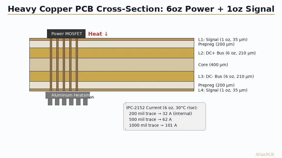
Practical Current Capacity Table (30°C Rise, Still Air)
For internal layers at 30°C temperature rise above ambient:
| Trace Width | 3 oz Current | 6 oz Current | 10 oz Current |
|---|---|---|---|
| 100 mil | 12 A | 19 A | 28 A |
| 200 mil | 20 A | 32 A | 47 A |
| 500 mil | 38 A | 62 A | 91 A |
| 1000 mil | 62 A | 101 A | 148 A |
External layers carry approximately 20-30% more current due to better convection cooling.
The Cross-Section Formula
Current capacity depends on conductor cross-sectional area:
Area (mils²) = Width (mils) × Thickness (mils)
I_max ≈ k × Area^0.725 × ΔT^0.44
Where k ≈ 0.048 for internal layers and k ≈ 0.065 for external layers (IPC-2152 coefficients).
Bus Bar Integration: Embedded vs. External
Traditional power electronics use external copper bus bars bolted or soldered to the PCB. Embedded bus bar technology eliminates this by incorporating thick copper planes directly into the PCB stackup.
Advantages of Embedded Bus Bars
- Reduced parasitic inductance — Shorter current paths with tighter layer-to-layer spacing reduce loop inductance by 50-80% compared to external bus bars
- Better thermal management — Copper planes conduct heat laterally across the entire board area
- Higher reliability — Eliminates solder joints and mechanical connections that fatigue under thermal cycling
- Compact form factor — No standoff height required for external conductors
- Lower assembly cost — Fewer discrete components and mounting hardware
Embedded Bus Bar Stackup Design
A typical 6-layer embedded bus bar stackup for a 3-phase inverter:
L1: Signal + gate drives (1 oz)
L2: DC+ bus plane (10 oz)
L3: DC– bus plane (10 oz)
L4: Phase A output (6 oz)
L5: Phase B output (6 oz)
L6: Signal + control (1 oz)
The DC+ and DC– planes sit adjacent with only a thin dielectric between them (50-100 µm), creating a low-inductance DC bus capacitor structure.
Need Heavy Copper PCBs for Your Power Design?
AtlasPCB manufactures 3-20 oz copper PCBs with embedded bus bars. Get DFM review within 24 hours.
Request a Quote →Thermal Management in Heavy Copper Designs
Heavy copper itself acts as a heat spreader, but proper thermal design requires additional strategies.
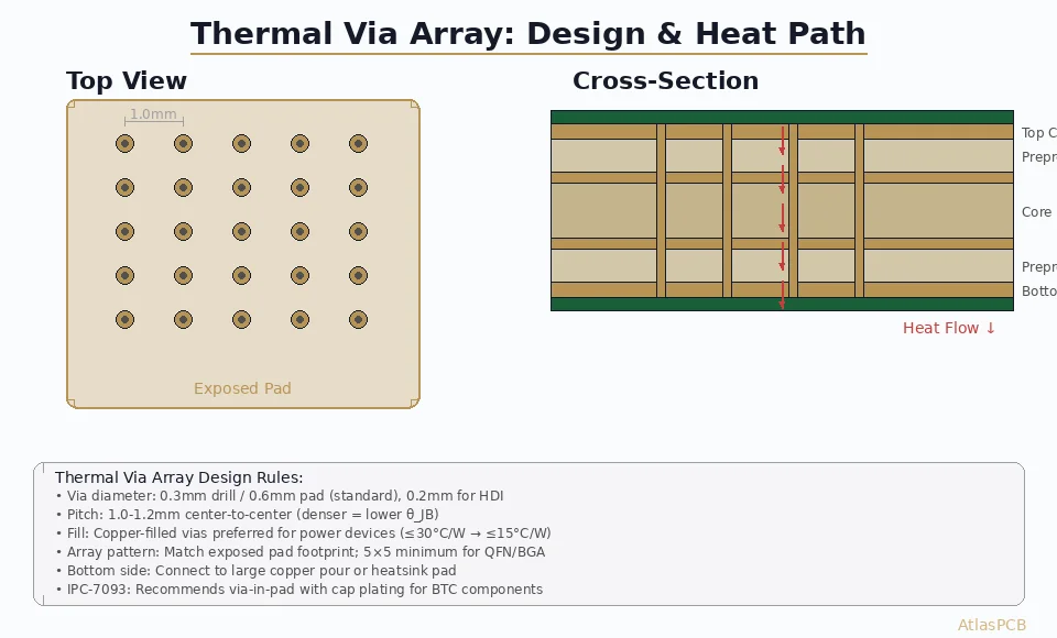
Thermal Via Arrays
Thermal vias transfer heat from hot components to internal copper planes or the bottom-side heatsink:
- Via diameter: 0.3-0.5 mm (larger = lower thermal resistance)
- Via pitch: 1.0-1.5 mm grid pattern
- Fill: Copper-filled vias offer 3-4× better thermal conductivity than hollow vias
- Array sizing: Cover the entire component thermal pad area plus 1-2 mm margin
A single 0.3 mm copper-filled via has approximately 50°C/W thermal resistance through a 1.6 mm board. An array of 25 vias (5×5) reduces this to ~2°C/W.
Coin/Slug Integration
For extreme thermal loads (>50 W per component), copper coins (solid copper slugs) can be press-fit or soldered into the PCB:
- Coin thickness: typically 1.0-3.0 mm
- Thermal resistance: <0.5°C/W for a 10×10 mm coin
- Must be co-planar with pad surface (±50 µm tolerance)
- Requires special tooling in manufacturing
Heat Spreading Calculations
Effective thermal spreading depends on copper coverage area and thickness:
R_spread ≈ 1 / (k_Cu × A_Cu / t_board)Where k_Cu = 385 W/m·K, A_Cu is the copper area, and t_board is the board thickness.
For a 6 oz copper plane covering 50 cm²:
R_spread ≈ 1 / (385 × 50×10⁻⁴ / 1.6×10⁻³) = 0.83°C/WDesign Rules for Heavy Copper
Manufacturing heavy copper requires wider clearances and different etching parameters.
Minimum Spacing (Copper-to-Copper)
| Copper Weight | Min Trace/Space | Min Annular Ring |
|---|---|---|
| 3 oz | 8/8 mil | 6 mil |
| 6 oz | 12/12 mil | 8 mil |
| 10 oz | 16/16 mil | 10 mil |
| 20 oz | 25/25 mil | 15 mil |
Etching Considerations
Heavy copper etching creates trapezoidal trace profiles due to isotropic etch undercutting:
- Etch factor for 6 oz: ~3:1 (undercut = thickness/3 per side)
- A 6 oz trace designed at 12 mil will have ~9 mil at the base after etching
- Account for this by adding 2× (thickness/etch_factor) to trace widths
Via Design for Heavy Copper
- Minimum drill size increases with copper weight (0.3 mm for 3 oz → 0.5 mm for 10 oz)
- Aspect ratio limited to 8:1 for reliable plating
- Back-drill may be needed for signal integrity on mixed heavy/standard stackups
- PTH copper plating: minimum 25 µm (1 oz) in barrel regardless of surface copper weight
Manufacturing Process Differences
Plating vs. Etching
Two approaches for creating heavy copper patterns:
Subtractive (Etch-down):
- Start with thick copper foil
- Etch away unwanted areas
- Better for simple patterns with large features
- Limited by etch factor at >6 oz
Pattern Plating (Additive):
- Start with thin base copper (0.5-1 oz)
- Plate up to target thickness in pattern areas
- Better edge definition (straighter walls)
- Preferred for 6+ oz with tight features
- More expensive but superior quality
Lamination Challenges
Thick copper creates fill challenges during lamination:
- Resin must flow to fill the gap between traces (height = copper thickness)
- Prepreg selection critical: high-resin-content materials (>65% RC)
- Multiple lamination cycles may be needed for >10 oz
- Press cycle must be optimized to avoid voiding while ensuring copper does not shift
Registration and Dimensional Stability
Heavy copper causes material movement during thermal processing:
- CTE mismatch between copper and laminate creates stress
- Use balanced copper distribution (symmetric stackup)
- Tie copper areas with cross-hatch patterns to reduce stress concentration
- Allow ±3 mil registration tolerance for 6 oz+ layers
Application Examples
Electric Vehicle Inverter (400V/500A)
- Stackup: 10-layer with 10 oz bus planes
- Current per phase: 160 A RMS
- Bus bar planes: DC+ and DC– on L3/L4
- Thermal management: Copper-filled via arrays + aluminum baseplate
- Operating temperature: -40°C to +125°C
Industrial Motor Drive
- Stackup: 8-layer, 6 oz power + 1 oz signal
- IGBTs mounted on embedded copper coins
- Parasitic inductance target: <5 nH per switching loop
- Board size: 200 × 150 mm
- Power dissipation: 80 W total
Telecom Power Supply (48V/100A)
- Stackup: 6-layer with 4 oz copper
- Multi-phase buck converter with interleaved phases
- Thermal via arrays under each MOSFET
- Operating efficiency: >96% at full load
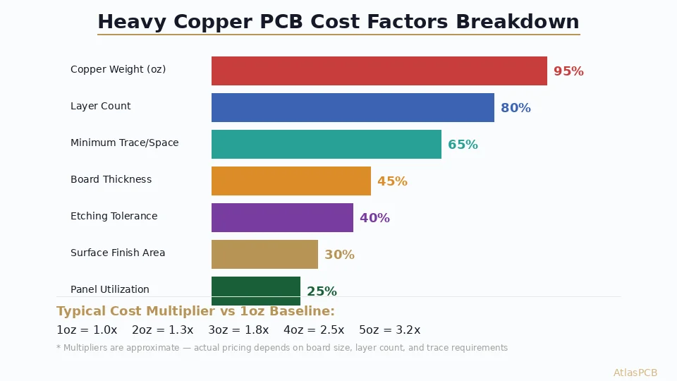
Cost Considerations
Heavy copper PCBs cost significantly more than standard boards:
| Factor | Impact |
|---|---|
| Copper material | 3-10× raw material cost |
| Etching time | 3-5× longer processing |
| Drill wear | 2-3× more frequent bit changes |
| Lamination | Special prepreg, longer press cycles |
| Plating | Higher current/time for via fill |
| Yield | Lower yield on tight-tolerance designs |
Rule of thumb: A 6 oz heavy copper board costs roughly 3-4× a standard 1 oz board of the same size and layer count.
Cost Optimization Strategies
- Use heavy copper only where needed — Mix 6 oz power layers with 1 oz signal layers
- Maximize copper area — Large copper pours etch faster and more uniformly
- Relax tolerances — Allow 12/12 mil minimum instead of 8/8 mil
- Panel utilization — Rectangular boards pack better, reducing waste
- Design for the process — Consult your fabricator’s DFM guidelines early
Further Reading
- Thermal Via Array Design Rules for Power Electronics
- PCB Design for GaN and SiC Power Devices
- Copper Coin Thermal Management for High-Power PCBs
- What Causes PCB Delamination
Ready to prototype your power electronics PCB? AtlasPCB specializes in heavy copper fabrication from 3 oz to 20 oz, including embedded bus bar designs and copper-filled thermal vias. Get a quote today or explore our power electronics capabilities.
About AtlasPCB — We specialize in complex PCB manufacturing for HDI, RF, and high-reliability applications. Explore our heavy copper PCB manufacturing, or get an aluminum and metal-core PCB services . Every order includes free engineering review. Get your quote.
Reviewed by AtlasPCB Engineering Team — IPC-certified manufacturing specialists with 15+ years of production experience in HDI, RF, and high-reliability PCB fabrication. Content based on factory floor data and real customer design reviews.
- heavy copper
- power electronics
- PCB design
- bus bar
- thermal management
- high current
- copper weight