· AtlasPCB Engineering · Engineering · 12 min read
PCB Via Transitions in RF Design: Coaxial Via, GCPW, and Antipad Optimization for mmWave Signals
Master RF via transitions from microstrip to stripline. Learn coaxial via structures, GCPW launch design, antipad sizing, and ground stitching techniques for minimal signal loss at 5G and mmWave frequencies.
Why RF Via Transitions Matter
Every RF signal path that changes layers in a multilayer PCB must pass through a via transition. At low frequencies, vias are electrically invisible — a simple plated-through hole introduces negligible reflection. But as operating frequencies climb into the gigahertz and millimeter-wave range, the via structure becomes a critical impedance discontinuity that can make or break your design.
At 28 GHz (5G NR FR2) or 77 GHz (automotive radar), a poorly designed via transition can introduce 1–3 dB of insertion loss and return loss worse than −10 dB. In a signal chain with multiple layer transitions — microstrip to stripline to microstrip — these losses compound rapidly, degrading link budget and increasing bit error rates.
The solution is to treat every RF via transition as a controlled-impedance transmission line segment. This article covers the three key techniques: coaxial via structures, GCPW (Grounded Coplanar Waveguide) launch pads, and antipad optimization — the engineering toolkit for low-loss layer transitions at mmWave frequencies.
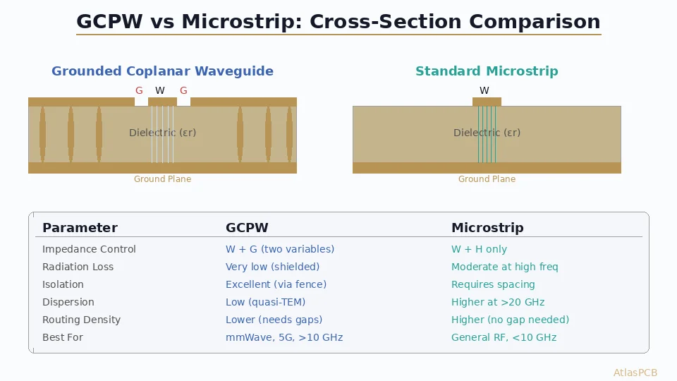
Understanding Via Impedance Discontinuity
The Problem with Standard Vias at RF
A standard plated-through hole in a PCB is a cylindrical conductor surrounded by dielectric material and ground planes. Its characteristic impedance depends on:
- Via barrel diameter (drill size + plating)
- Antipad (clearance) diameter in each ground/power plane
- Dielectric constant of the surrounding laminate
- Proximity to ground (other vias, planes)
For a typical FR-4 board with a 0.3 mm drill via and default 0.5 mm antipads, the via impedance is often 70–100 Ω — far above the 50 Ω target for most RF systems. This impedance mismatch creates reflections at every layer transition.
Impedance Formula for Via Structures
The characteristic impedance of a via can be approximated using the coaxial transmission line formula:
Z₀ = (60 / √εᵣ) × ln(D_antipad / D_via)
Where:
- Z₀ is the characteristic impedance (target: 50 Ω)
- εᵣ is the effective dielectric constant
- D_antipad is the antipad diameter
- D_via is the via pad diameter
For 50 Ω with εᵣ = 3.5 (typical mid-range laminate):
D_antipad / D_via ≈ 2.7
This ratio is the foundation of all RF via transition design.
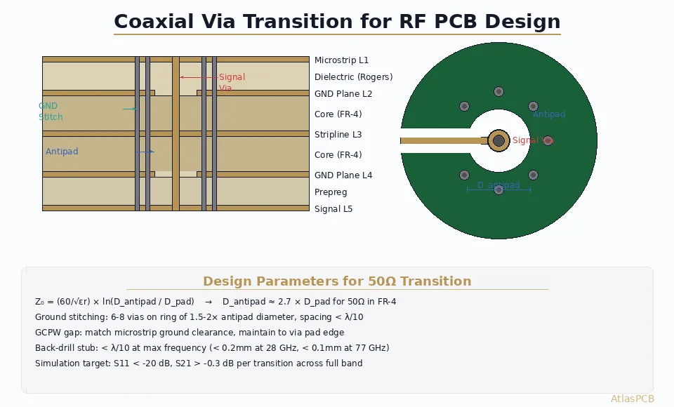
Coaxial Via Structure Design
Anatomy of a Coaxial Via
A coaxial via structure consists of three elements working together:
Signal via — The center conductor carrying the RF signal through the stackup. Uses the smallest reliable drill size (typically 0.2–0.3 mm for HDI, 0.3–0.4 mm for standard).
Antipad — The clearance hole in each ground and power plane layer. Sized to achieve 50 Ω impedance using the coaxial formula above.
Ground stitching vias — A ring of vias surrounding the signal via, connecting all ground planes. These form the outer conductor of the coaxial structure.

Design Rules for Coaxial Vias
Signal via sizing:
- Drill diameter: 0.2–0.3 mm (laser) or 0.3–0.4 mm (mechanical)
- Pad diameter: drill + 0.15–0.2 mm (minimum annular ring per IPC-6012)
- Back-drill stub if via extends beyond the target stripline layer (stub length < λ/10)
Antipad diameter:
- Start with D_antipad = 2.7 × D_pad for 50 Ω in FR-4 (εᵣ ≈ 4.2)
- For low-loss laminates (εᵣ ≈ 3.0–3.5): D_antipad = 2.5 × D_pad
- For Rogers RO4350B (εᵣ = 3.48): D_antipad ≈ 2.6 × D_pad
- Verify with 3D EM simulation — the formula is a starting point, not the final answer
Ground stitching vias:
- Minimum 4 vias equally spaced around the signal via
- Place on a circle of diameter ≈ 1.5–2× antipad diameter
- Via-to-via spacing < λ/10 at the highest frequency of interest
- Connect ALL ground planes in the stackup (not just adjacent layers)
Worked Example: 28 GHz Coaxial Via
Target: Microstrip-to-stripline transition on Rogers RO4350B + FR-4 hybrid stackup, 50 Ω, 28 GHz
Step 1 — Signal via: 0.25 mm drill, 0.45 mm pad
Step 2 — Antipad: 2.6 × 0.45 mm = 1.17 mm → round to 1.2 mm diameter
Step 3 — Ground vias: λ at 28 GHz in εᵣ=3.48 ≈ 5.75 mm. Spacing < 0.575 mm. Place 6 ground vias on a 2.0 mm diameter circle → spacing = π × 2.0 / 6 = 1.05 mm. This exceeds λ/10 — increase to 8 vias → spacing = 0.785 mm. Still slightly over. Reduce circle to 1.8 mm diameter with 8 vias → spacing = 0.707 mm. Acceptable for 28 GHz with margin.
Step 4 — Back-drill: If the signal enters on layer 1 (microstrip) and transitions to layer 3 (stripline), back-drill from bottom to remove the stub below layer 3. Target stub length < 0.2 mm (λ/10 at 28 GHz ≈ 0.58 mm).
Step 5 — Simulate: Run 3D EM simulation (HFSS or CST) to verify S11 < −20 dB and S21 > −0.3 dB across the 24.25–29.5 GHz band.
GCPW Launch Pad Design
What Is a GCPW Launch?
A Grounded Coplanar Waveguide (GCPW) launch is a transitional structure that connects a microstrip or stripline trace to the via transition. Instead of abruptly ending the trace at the via pad, a GCPW launch gradually modifies the electromagnetic field pattern to match the coaxial via structure.
The GCPW launch consists of:
- Signal trace tapering into the via pad
- Coplanar ground cutouts on the same layer as the signal trace
- Ground vias connecting the coplanar ground to internal ground planes
Why GCPW Launches Improve Performance
A microstrip trace has its electric field concentrated between the trace and the ground plane below. A via structure has its field distributed radially (like a coaxial cable). The transition between these field configurations causes mode conversion and radiation — both sources of loss.
A GCPW launch solves this by:
- Introducing coplanar ground reference near the signal trace, creating a hybrid microstrip/coplanar mode
- Gradually transitioning the field configuration from planar to radial
- Providing a low-impedance return current path directly adjacent to the signal via
GCPW Launch Design Rules
Coplanar gap width: Set equal to the microstrip trace spacing to ground (typically 0.15–0.25 mm for 50 Ω on thin dielectrics). Maintain constant gap width from trace to via pad.
Taper geometry: If the via pad is wider than the trace, taper the trace linearly over a length of 0.5–1.0 mm. A linear taper is sufficient below 40 GHz; above 40 GHz, consider a Klopfenstein or exponential taper profile.
Coplanar ground extent: Extend coplanar ground at least 3× the gap width on each side of the signal trace. Connect to the internal ground plane with stitching vias every λ/10.
Launch pad shape: The via pad can be elongated (oval or rounded rectangle) in the direction of the incoming trace to reduce the impedance discontinuity at the pad transition.
Need RF PCB Manufacturing with Tight Impedance Control?
AtlasPCB delivers ±5% impedance tolerance on Rogers, Megtron, and hybrid stackups with TDR verification on every panel.
Get a Quote →Antipad Optimization Techniques
Non-Uniform Antipads
In a multilayer stackup, not every ground plane layer requires the same antipad diameter. The signal via only needs a controlled-impedance antipad in the layers where it is actively carrying an RF signal. On layers where the via passes through but the signal has already transitioned to a trace, the antipad can be reduced to the minimum fabrication clearance.
Strategy:
- Active transition layers (where the signal enters/exits the via): Full-size antipad for 50 Ω impedance
- Pass-through layers (via stub region, if not back-drilled): Minimum antipad (just enough for fabrication clearance)
- Non-functional pads: Remove entirely on pass-through layers to reduce capacitive loading
This technique is especially important for thick boards (>8 layers) where the via passes through many plane layers.
Antipad Shape Optimization
Circular antipads are standard, but non-circular shapes can improve performance:
Oval/elongated antipads: Extend the antipad in the direction of the connected trace to reduce the impedance step at the pad-to-trace junction. Typical aspect ratio: 1.3:1 to 1.5:1.
Stadium-shaped antipads: Combine a circular antipad at the via with a rectangular channel extending toward the trace breakout. This gradually transitions from the coaxial impedance to the stripline impedance.
Simulation-driven shapes: At frequencies above 40 GHz, custom antipad shapes optimized through parametric EM simulation can recover 0.5–1.0 dB of insertion loss compared to standard circular antipads.
Antipad Interactions in Dense Via Fields
When multiple signal vias are placed close together (as in a connector footprint or BGA breakout), their antipads interact. Adjacent antipads that overlap or nearly touch create unexpected impedance variations:
- Merging antipads: If two antipads overlap, the combined clearance lowers the impedance of both vias below the target. Increase via pitch or reduce antipad diameter.
- Ground plane fragmentation: Many closely-spaced antipads can fragment the ground plane, creating return current detours and increasing inductance. Maintain minimum 0.2 mm copper web between adjacent antipads.
- Differential via pairs: For differential signals, the antipad geometry must maintain symmetry between the positive and negative vias. A shared oval antipad for the pair can improve differential impedance control.
Ground Stitching Via Strategies
Via Fence for Isolation
Beyond supporting impedance control at via transitions, ground stitching vias serve a second purpose: electromagnetic isolation. A row of stitching vias between adjacent RF signal vias or between RF and digital sections creates a via fence that attenuates coupling.
Via fence design:
- Via spacing: < λ/20 for >20 dB isolation at the operating frequency
- Single row: 15–20 dB isolation typical
- Double row (staggered): 30–40 dB isolation
- Triple row: >40 dB isolation (required for TX/RX isolation in radar modules)
Stitching Via Placement Near Transitions
Around each RF via transition, ground stitching vias should be placed at two zones:
- Immediate ring (coaxial structure): 4–8 vias at 1.5–2× antipad radius, connecting all ground planes
- Guard ring (isolation): Additional vias at 2–3× the immediate ring radius, spaced < λ/10, particularly important between the via transition and any nearby digital signals or power planes
Common Mistakes in Ground Via Placement
- Insufficient depth: Stitching vias that only connect two adjacent ground planes instead of all planes leave return current paths incomplete. Use through-hole vias or ensure buried vias span all relevant ground layers.
- Asymmetric placement: Uneven distribution of ground vias around the signal via creates asymmetric field patterns, converting differential mode to common mode in differential pairs.
- Missing vias at layer changes: Every point where a ground plane changes (split plane boundary, power plane cutout) needs stitching vias to maintain low-impedance return path continuity.
Practical Design Flow
Step-by-Step RF Via Transition Design
Define requirements: Operating frequency, bandwidth, target impedance, maximum allowable insertion loss and return loss per transition.
Select via technology: Mechanical drill (≥0.2 mm), laser drill (<0.15 mm), or combination. Smaller vias have less parasitic inductance and capacitance but cost more.
Calculate initial antipad: Use the coaxial formula Z₀ = (60/√εᵣ) × ln(D_antipad/D_via) and solve for D_antipad.
Place ground stitching vias: Start with 6 vias on a circle, verify spacing < λ/10.
Design GCPW launch: Add coplanar ground cutouts and taper the trace into the via pad.
Back-drill or HDI: Determine if via stubs need removal. For frequencies > 10 GHz, back-drilling is almost always required unless using blind/buried vias.
Simulate: 3D EM simulation of the complete transition structure. Optimize antipad diameter, stitching via positions, and launch geometry to meet spec.
DFM check: Verify all dimensions are within the fabrication house’s capability. Discuss antipad tolerances and back-drill depth control with your PCB manufacturer.
DFM Considerations for RF Vias
Work closely with your PCB fabricator on these critical manufacturing constraints:
- Antipad tolerance: Typical registration accuracy is ±50 μm for inner layers. Your antipad must accommodate this tolerance without creating impedance violations.
- Back-drill depth tolerance: Most fabricators achieve ±100–150 μm. For thick boards at high frequencies, this may be insufficient — consider controlled-depth blind vias instead.
- Plating uniformity: Via barrel plating thickness affects the effective via diameter. Specify plating thickness tolerance (typically ±5 μm for standard, ±3 μm for precision).
- Laminate registration: On [hybrid stackups using Rogers and FR-4]/blog/pcb-hybrid-stackup-rogers-fr4/), material CTE mismatch can cause layer-to-layer misregistration. Discuss panel registration marks and coupon placement with the fab.
Frequency-Specific Guidelines
Sub-6 GHz (5G NR FR1, Wi-Fi 6E)
At these frequencies, standard vias with modest optimization perform well:
- Standard 0.3 mm drill vias are acceptable
- Antipad sizing per the coaxial formula is sufficient — simulation optional
- 4 ground stitching vias around each signal via
- Back-drilling usually not required for boards < 2 mm thick
- GCPW launch is beneficial but not critical
24–30 GHz (5G NR FR2, K-band Radar)
This range demands careful transition design:
- Prefer 0.2–0.25 mm drill vias (laser or small mechanical)
- Full coaxial via structure with 6–8 ground stitching vias
- Back-drilling mandatory for any via stub > 0.3 mm
- GCPW launch strongly recommended
- Antipad must be simulation-verified
- Consider [low-loss laminates like Megtron 7]/blog/mmwave-pcb-material-selection-rogers-megtron-lcp-5g-6g/) for reduced dielectric loss
60–77 GHz (V-band, Automotive Radar)
Millimeter-wave transitions require full optimization:
- Laser-drilled microvias (0.1–0.15 mm) preferred for minimum parasitic
- 8+ ground stitching vias with spacing < 0.3 mm
- Non-circular (optimized) antipad shapes from parametric simulation
- GCPW launch with Klopfenstein taper mandatory
- [HDI stackup with any-layer via]/blog/any-layer-hdi-pcb-design-wearable-sip/) architecture for shortest possible via transitions
- Consider embedded cavity or substrate-like PCB approaches for ultimate performance
Simulation and Validation
3D EM Simulation Setup
For accurate via transition simulation:
- Model the complete structure: trace approach, GCPW launch, via, antipad, stitching vias, and trace exit
- Include realistic material properties (frequency-dependent εᵣ and tan δ)
- Use wave ports or lumped ports matched to the trace impedance
- Simulate across the full operating bandwidth plus margin (2× for harmonic content)
- Extract S-parameters: target S11 < −20 dB, S21 > −0.3 dB per transition
TDR Verification in Fabrication
After manufacturing, validate via transitions using Time Domain Reflectometry (TDR):
- Design dedicated [test coupons]/blog/pcb-test-coupon-design-ipc-standards/) with via transitions matching the actual design
- TDR should show impedance within ±5 Ω of target through the transition
- If using [impedance-controlled stackups]/blog/controlled-impedance-pcb-design-stackup-calculations/), verify both trace impedance and via impedance on the same coupon
Further Reading
- [RF Microwave PCB Design Guidelines]/blog/rf-microwave-pcb-design/) — Complete RF design fundamentals
- [Rogers vs PTFE Material Selection for 5G]/blog/rf-pcb-rogers-vs-ptfe-material-selection-5g/) — Choosing the right RF laminate
- [PCB Back-Drilling for Via Stub Removal]/blog/pcb-back-drilling-via-stub-removal-signal-integrity/) — Detailed back-drill process guide
- [mmWave PCB Material Selection: Rogers, Megtron, LCP]/blog/mmwave-pcb-material-selection-rogers-megtron-lcp-5g-6g/) — Material comparison for high-frequency applications
- [Controlled Impedance PCB Design and Stackup Calculations]/blog/controlled-impedance-pcb-design-stackup-calculations/) — Impedance design fundamentals
Need help designing RF via transitions for your next mmWave or 5G PCB? AtlasPCB’s engineering team reviews every RF design for manufacturing feasibility, impedance accuracy, and material compatibility. Request a free design review →
About AtlasPCB — We specialize in complex PCB manufacturing for HDI, RF, and high-reliability applications. Explore our RF and high-frequency PCB services, or get an impedance-controlled PCB manufacturing . Every order includes free engineering review. Get your quote.
Reviewed by AtlasPCB Engineering Team — IPC-certified manufacturing specialists with 15+ years of production experience in HDI, RF, and high-reliability PCB fabrication. Content based on factory floor data and real customer design reviews.
- rf-pcb
- via-transition
- microstrip
- stripline
- gcpw
- coaxial-via
- antipad
- mmwave
- 5g
- signal-integrity