· AtlasPCB Engineering · Engineering · 13 min read
PCB Power Integrity and Decoupling: Complete PDN Design Guide for High-Speed Digital Systems
Master Power Distribution Network design with target impedance calculations, decoupling capacitor selection strategies, and PDN simulation techniques for FPGA, SoC, and high-speed digital PCBs.

PCB Power Integrity and Decoupling: Complete PDN Design Guide
Power integrity (PI) has become the dominant design challenge in modern high-speed PCBs. As core voltages drop below 1.0V while transient currents exceed 50A in advanced FPGAs and SoCs, the Power Distribution Network (PDN) must deliver stable, low-noise power with milliohm-level impedance across a bandwidth spanning DC to several GHz. A poorly designed PDN doesn’t just cause power rail noise — it creates simultaneous switching noise (SSN) that degrades [signal integrity]/blog/signal-integrity-pcb-design-guide/), increases bit error rates, and can make an otherwise sound design non-functional.
This guide covers the complete PDN design methodology: target impedance calculation, decoupling capacitor network design, power plane optimization, PDN resonance analysis, and simulation-driven verification using industry-standard tools.
Understanding the Power Distribution Network
The PDN is the complete electrical path from the voltage regulator module (VRM) output to the IC power pins. It includes:
- Voltage Regulator Module (VRM): Provides regulated DC voltage with finite output impedance and bandwidth (typically effective up to 10-50kHz)
- Bulk capacitors: 10-470μF electrolytic or polymer capacitors near the VRM, effective from ~1kHz to ~1MHz
- Mid-frequency decoupling capacitors: 100nF-1μF MLCC capacitors distributed across the board, effective from ~1MHz to ~100MHz
- High-frequency decoupling capacitors: 1nF-100nF MLCC capacitors placed directly at IC power pins, effective from ~100MHz to ~1GHz
- Power/ground plane pairs: PCB copper planes that provide distributed planar capacitance effective above ~500MHz
- Via interconnects: Vertical connections between planes and capacitor pads
- IC package: Bond wires/bumps and internal power distribution with parasitic inductance
Each element dominates the PDN impedance in a specific frequency band. The design challenge is ensuring a smooth, low-impedance transition between these bands with no resonant peaks that exceed the target impedance.
Target Impedance: The Foundation of PDN Design
The Target Impedance Formula
Target impedance defines the maximum allowable PDN impedance at any frequency:
Z_target = ΔV / ΔI
Where:
- ΔV = allowable voltage ripple = V_supply × ripple_percentage
- ΔI = maximum transient current demand
Worked Example: Xilinx Kintex UltraScale FPGA
Consider a Kintex UltraScale XCKU115 with the following power rails:
VCCINT (0.95V core):
- Ripple tolerance: ±3% → ΔV = 0.95V × 0.03 = 28.5mV
- Maximum transient current: 25A
- Z_target = 28.5mV / 25A = 1.14mΩ
VCCO (1.8V I/O bank):
- Ripple tolerance: ±5% → ΔV = 1.8V × 0.05 = 90mV
- Maximum transient current: 8A
- Z_target = 90mV / 8A = 11.25mΩ
VCCAUX (1.8V auxiliary):
- Ripple tolerance: ±5% → ΔV = 1.8V × 0.05 = 90mV
- Maximum transient current: 3A
- Z_target = 90mV / 3A = 30mΩ
The 1.14mΩ target for VCCINT is extremely challenging — this drives the need for closely-spaced plane pairs, extensive decoupling networks, and careful via design. This is why high-performance [multilayer PCB stackup design]/blog/pcb-stackup-design-guide/) is critical for power integrity.
Frequency Range Considerations
The target impedance must be met from DC up to the maximum frequency of concern:
f_max = 1 / (π × t_rise)
For a signal with 100ps rise time: f_max = 1 / (π × 100ps) = 3.18 GHz
This means the PDN impedance must remain below Z_target from DC to over 3GHz — a range spanning nearly 10 decades of frequency.
Decoupling Capacitor Network Design
The Three-Tier Decoupling Strategy
Effective decoupling requires a coordinated network of capacitors, each optimized for a specific frequency band:
Tier 1 — Bulk Decoupling (DC to ~1MHz):
- Values: 10μF to 470μF
- Types: Polymer aluminum, tantalum polymer, or high-capacitance MLCC
- Quantity: 2-6 per power rail
- Placement: Near VRM output, within 25mm
- Purpose: Provide charge reservoir for sustained current draw, bridge VRM bandwidth limitation
Tier 2 — Mid-Frequency Decoupling (1MHz to ~200MHz):
- Values: 100nF to 1μF
- Types: X7R or X5R MLCC, 0402 or 0201 package
- Quantity: 10-40 per major power rail
- Placement: Distributed across the IC footprint area, within 10mm of power pins
- Purpose: Supply charge for medium-frequency transients, fill the impedance gap between bulk caps and high-frequency caps
Tier 3 — High-Frequency Decoupling (200MHz to ~2GHz):
- Values: 1nF to 100nF
- Types: C0G/NP0 MLCC for lowest ESR, 0201 or 01005 package
- Quantity: 20-80+ per major power rail
- Placement: Directly at IC power pins, within 2mm, on same layer or immediately adjacent via
- Purpose: Suppress high-frequency switching noise at the point of demand
Capacitor Self-Resonant Frequency (SRF)
Every real capacitor has a self-resonant frequency where it transitions from capacitive to inductive behavior:
SRF = 1 / (2π × √(L_ESL × C))
Below the SRF, the capacitor acts as intended. Above the SRF, it behaves as an inductor and is ineffective for decoupling. This is why you need multiple capacitor values — their SRFs are staggered to provide continuous low impedance across the frequency spectrum.
Typical SRFs for common MLCC packages:
| Value | Package | ESL (pH) | SRF (MHz) |
|---|---|---|---|
| 100μF | 1210 | 900 | 0.5 |
| 10μF | 0805 | 700 | 1.9 |
| 1μF | 0402 | 450 | 7.5 |
| 100nF | 0402 | 450 | 24 |
| 100nF | 0201 | 250 | 32 |
| 10nF | 0201 | 250 | 100 |
| 1nF | 0201 | 250 | 318 |
Anti-Resonance: The Hidden PDN Killer
When two capacitors with different SRFs are connected in parallel, they create an anti-resonant peak at a frequency between their individual SRFs. At anti-resonance, the impedance can spike far above the target impedance, potentially causing power rail oscillation.
The anti-resonant frequency occurs where the inductance of the larger capacitor (above its SRF) resonates with the capacitance of the smaller capacitor (below its SRF):
f_anti = 1 / (2π × √(L_ESL1 × C2))
Mitigation strategies:
- Use many capacitors of the same value (paralleling reduces ESR/ESL without creating new anti-resonances)
- Choose capacitor values with SRFs spaced no more than a decade apart
- Add damping resistance (0.5-2Ω) in series with bulk capacitors
- Verify with PDN simulation — never design by rule of thumb alone

Power Plane Design and Optimization
Closely-Spaced Plane Pairs: Your Best High-Frequency Decoupling
Above 500MHz, discrete capacitors become increasingly ineffective due to mounting inductance. The power/ground plane pair itself becomes the primary decoupling mechanism through distributed planar capacitance.
The capacitance of a plane pair is:
C_plane = ε₀ × εr × A / d
Where:
- ε₀ = 8.854 × 10⁻¹² F/m
- εr = dielectric constant (4.2 for FR-4, 3.5-3.8 for low-loss materials)
- A = overlapping plane area
- d = dielectric thickness between planes
Design guideline per IPC-2141: For optimal high-frequency PDN performance, use power/ground plane pairs with ≤100μm (4mil) dielectric spacing. Premium designs targeting sub-2mΩ impedance above 1GHz should use 50μm (2mil) or even 25μm (1mil) spacing.
| Dielectric Thickness | Capacitance (FR-4, 100cm²) | Z at 1GHz |
|---|---|---|
| 200μm (8mil) | 1.86nF | ~85mΩ |
| 100μm (4mil) | 3.72nF | ~43mΩ |
| 50μm (2mil) | 7.44nF | ~21mΩ |
| 25μm (1mil) | 14.88nF | ~11mΩ |
This is why [advanced stackup design]/blog/pcb-stackup-design-guide/) places power/ground plane pairs on adjacent layers with the thinnest available prepreg — it’s the most effective way to achieve low PDN impedance above 500MHz.
Current-Carrying Capacity: IPC-2152 Compliance
Power planes must carry substantial DC and AC current without excessive temperature rise. IPC-2152 supersedes the older IPC-2221 charts and uses a more accurate thermal model.
IPC-2152 key parameters for internal planes:
| Current (A) | Min. Copper Width for 10°C Rise (1oz) | Min. Copper Width for 20°C Rise (1oz) |
|---|---|---|
| 5 | 2.0mm | 1.2mm |
| 10 | 6.5mm | 3.8mm |
| 20 | 18mm | 10.5mm |
| 30 | 35mm | 20mm |
For high-current rails (>10A), consider using 2oz copper weight on power planes. The relationship between copper weight and current capacity is not linear — doubling copper thickness increases current capacity by approximately 40% for the same temperature rise, not 100%.
Voltage drop calculation: The DC voltage drop across a power plane is often overlooked but critical for low-voltage rails:
V_drop = I × R_sheet × L / W
Where R_sheet is the sheet resistance (0.49mΩ/sq for 1oz copper at 25°C, scaling to ~0.64mΩ/sq at 85°C). For a 1.0V rail carrying 20A across a 50mm plane with 30mm effective width in 1oz copper:
V_drop = 20A × 0.49mΩ × (50/30) = 16.3mV (1.63%)
This already consumes a significant portion of the ±3% budget, leaving minimal headroom for AC ripple.
Power Plane Splits and Isolation
Multi-rail PDN designs for FPGAs and SoCs require separate voltage domains on shared layers. When splitting power planes:
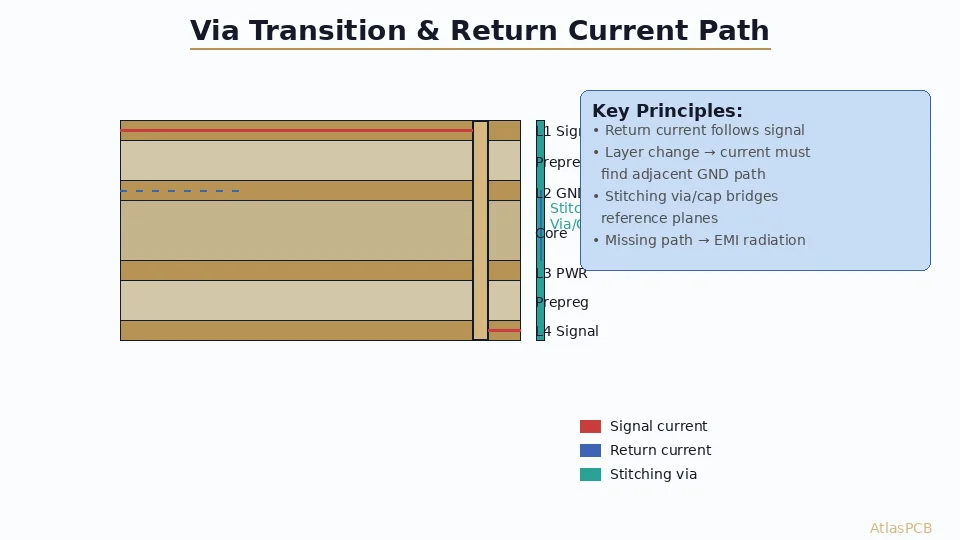
- Maintain a continuous ground plane: Never split the ground reference. Use dedicated, uninterrupted ground plane layers. This is fundamental to proper [grounding techniques]/blog/pcb-grounding-techniques/) for power integrity.
- Route signals away from split boundaries: Signals crossing a power plane split lose their return path reference, creating EMI and crosstalk
- Keep split gaps narrow: 20-50mil gaps are typical; wider gaps waste routing area
- Use stitching capacitors at split boundaries: 100nF capacitors at 5-10mm intervals provide AC continuity between voltage domains
Via Design for Power Distribution
Via Current Capacity
Per IPC-2221, a single plated-through via (0.3mm drill, 25μm plating) can carry approximately 1.5A with a 10°C temperature rise. High-current power connections require multiple vias:
| Current Required | Minimum Vias (0.3mm, 25μm plating) |
|---|---|
| 5A | 4 |
| 10A | 7 |
| 20A | 14 |
| 30A | 20 |
Via Inductance and PDN Impact
Every via adds parasitic inductance to the PDN path. A typical through-hole via (0.3mm drill, 1.6mm board) has approximately 0.5-1.0nH of inductance. For a decoupling capacitor connected through two vias (power + ground), the total added inductance is 1-2nH.
At 100MHz, 1nH of inductance creates an impedance of: Z_L = 2π × 100MHz × 1nH = 0.63Ω
This is orders of magnitude above a typical target impedance of 2mΩ! This is why high-frequency decoupling capacitor placement and via design is critical.
Via inductance reduction strategies:
- Use multiple vias per capacitor pad (2-3 vias per pad reduces inductance by 50-67%)
- Minimize via length — use blind/buried vias to connect to inner plane layers. Learn more about [via types and their applications]/blog/pcb-via-types-guide/)
- Place capacitor pads directly over via-in-pad connections
- Use via-in-pad with copper fill for BGA breakout areas
- Maintain close via-to-via spacing for power/ground via pairs (≤1mm)
Via Stitching for Power Plane Integrity
Via stitching connects power planes on different layers and prevents cavity resonance between plane pairs. Per IPC-2141 guidelines:
Stitching via spacing ≤ λ/20 at the maximum frequency of concern
For f_max = 3GHz in FR-4 (εr = 4.2): λ = c / (f × √εr) = 3×10⁸ / (3×10⁹ × √4.2) = 48.8mm
Maximum stitching via spacing = 48.8mm / 20 = 2.44mm
In practice, 2-3mm stitching via spacing is standard for multi-GHz designs. For [HDI PCBs]/blog/hdi-pcb-technology/) with microvias, even tighter spacing of 1-1.5mm is achievable and recommended for the most demanding PDN applications.
Cavity Resonance and Mitigation
What Causes Cavity Resonance?
Parallel power/ground plane pairs form a resonant cavity — essentially a rectangular waveguide. Resonant frequencies occur at:
f_mn = (c / 2√εr) × √((m/L)² + (n/W)²)
Where m,n are mode numbers (1,0), (0,1), (1,1), etc., and L, W are the plane dimensions.
For a 100mm × 80mm plane pair in FR-4:
- f_10 = 732MHz (first mode along length)
- f_01 = 915MHz (first mode along width)
- f_11 = 1.17GHz (diagonal mode)
At these resonant frequencies, the PDN impedance spikes dramatically, often exceeding the target impedance by 10-100×.
Cavity Resonance Mitigation
1. Via stitching around plane perimeter: Place ground vias at ≤λ/20 spacing around the board edge and around cutouts. This raises the fundamental resonant frequency and reduces Q-factor.
2. Embedded planar capacitance: Ultra-thin dielectric layers (25-50μm) push resonant peaks to higher frequencies where they are naturally damped by dielectric and conductor losses.
3. Shorting vias within the cavity: A grid of stitching vias across the plane area disrupts resonant modes. This is the most effective mitigation for designs with large uninterrupted plane areas.
4. Lossy dielectric materials: Higher-Df materials (Df > 0.015) provide natural resonance damping, though this contradicts the trend toward low-loss materials for [signal integrity]/blog/signal-integrity-pcb-design-guide/). The design trade-off must be evaluated for each application.
Multi-Rail PDN Design for FPGAs and SoCs
Modern FPGAs like Xilinx Versal or Intel Agilex have 10-20+ distinct power rails, each with different voltage, current, sequencing, and noise requirements:
| Rail Type | Typical Voltage | Max Current | Z_target | Priority |
|---|---|---|---|---|
| Core logic | 0.70-0.88V | 30-80A | 0.5-1.5mΩ | Critical |
| I/O banks | 1.2-3.3V | 5-15A | 5-20mΩ | High |
| Transceivers | 0.9-1.1V | 3-10A | 3-10mΩ | Critical |
| Auxiliary | 1.8V | 2-5A | 15-40mΩ | Medium |
| Configuration | 1.8/2.5V | 0.5-2A | 30-80mΩ | Low |
Design Hierarchy for Multi-Rail PDN
- Allocate dedicated plane pairs for the most critical rails (core, transceiver) with thinnest available dielectric
- Share planes for lower-current rails using plane splits with stitching capacitors at boundaries
- Place VRMs close to the FPGA — minimize the power delivery path length
- Sequence power rails per FPGA vendor requirements (typically core first, then I/O, then auxiliary)
- Simulate each rail independently and combined to catch inter-rail coupling effects
PDN Simulation and Verification
Frequency-Domain Analysis
PDN simulation tools calculate the impedance versus frequency at specific probe points (typically IC power pins). The primary output is the Z(f) plot — impedance magnitude versus frequency — which must remain below Z_target across the entire band.
Industry-standard tools:
- ANSYS SIwave: Full-wave 3D electromagnetic solver, gold standard for PDN analysis
- Keysight ADS (PathWave): Circuit and EM co-simulation, excellent for what-if analysis
- Cadence Sigrity PowerDC/PowerSI: Integrated with Allegro PCB flow
- Altium PDN Analyzer: Built into Altium Designer, accessible for mainstream designs
- Open-source: openEMS with custom scripts for academic/prototype work
Time-Domain Verification
Frequency-domain analysis alone may miss transient events. Time-domain simulation uses actual IC switching profiles (often from IBIS models) to predict:
- Peak voltage droop during burst switching
- Settling time after load transients
- Power rail ringing and overshoot
Measurement Validation
Post-fabrication PDN validation uses a 2-port VNA (Vector Network Analyzer) measurement:
- Connect Port 1 to a power via near the IC
- Connect Port 2 to a ground via adjacent to Port 1
- Measure S21 (transmission) and convert to impedance: Z = 2 × Z0 × 10^(S21_dB/20)
This provides the actual PDN impedance profile for correlation with simulation.
Practical Design Rules Summary
| Parameter | Design Rule | Reference |
|---|---|---|
| Target impedance | Z = ΔV/ΔI, verify flat from DC to f_max | — |
| Power/ground spacing | ≤100μm (4mil), prefer ≤50μm (2mil) | IPC-2141 |
| Via stitching pitch | ≤λ/20 at f_max | IPC-2141 |
| Decoupling cap placement | ≤2mm from IC power pin for HF caps | IPC-2141 |
| Power via current | ~1.5A per via (0.3mm, 25μm, 10°C rise) | IPC-2152 |
| Plane copper weight | ≥1oz for <10A, ≥2oz for >10A power planes | IPC-2152 |
| Bulk cap ESR | 5-20mΩ for damping anti-resonance | — |
| Cap mounting inductance | ≤0.5nH per pad (via-in-pad preferred) | — |
| Plane split gap | 20-50mil, with stitching caps at 5-10mm | — |
| Ground plane | Continuous, never split, dedicated layer(s) | IPC-2141 |
Common PDN Design Mistakes
- Using only one capacitor value: Creates anti-resonant peaks between VRM bandwidth and capacitor SRF
- Ignoring via inductance: Even 1nH per via connection makes high-frequency caps ineffective
- Placing decoupling caps too far from IC: Every millimeter adds ~1nH of trace inductance
- Splitting the ground plane: Destroys return path continuity and increases PDN loop inductance
- Inadequate copper weight for high-current rails: Causes DC voltage drop that eats into ripple budget
- Skipping PDN simulation: Rule-of-thumb design cannot achieve milliohm-level impedance targets reliably
- Forgetting [thermal management]/blog/pcb-thermal-management/): High-current VRM and plane areas generate significant heat that increases copper resistance
Conclusion
Power integrity is not an afterthought — it is a fundamental design constraint that must be addressed from the initial stackup definition through final layout verification. The key principles are straightforward: calculate your target impedance, design a coordinated decoupling network that covers the full frequency range, use closely-spaced power/ground plane pairs for high-frequency performance, and validate everything with simulation before committing to fabrication.
For complex multi-rail FPGA and SoC designs, PDN analysis should begin at the schematic stage and iterate through layout. The cost of a board respin due to power integrity failure far exceeds the investment in proper upfront PDN design and simulation.
At Atlas PCB, we routinely manufacture boards with 50μm dielectric power plane pairs, via-in-pad for BGA decoupling, and controlled impedance stackups optimized for both signal and power integrity. Our engineering team can review your [stackup design]/blog/pcb-stackup-design-guide/) and provide PDN recommendations before you finalize your layout.
Ready to start your project? Upload your Gerbers for a free engineering review, or talk to an engineer about your design requirements.
Further Reading
- [HDI PCB Design Guide: Stackup Rules, Via Structures & DFM Checklist]/blog/hdi-pcb-design-guide/)
- [Via-in-Pad Design: Filled, Capped, and Plated Over — Complete Guide]/blog/via-in-pad-design/)
- [Controlled Impedance PCB: Design, Stackup & Testing Explained]/blog/controlled-impedance-pcb/)
- [High-Speed PCB Design: Signal Integrity Essentials for Modern Electronics]/blog/high-speed-pcb-design/)
- [Multilayer PCB Stackup Design Guide: 8 to 30+ Layers Step by Step]/blog/multilayer-pcb-stackup-design-guide/)
About AtlasPCB — We specialize in complex PCB manufacturing for HDI, RF, and high-reliability applications. Explore our impedance-controlled PCB manufacturing . Every order includes free engineering review. Get your quote.
Reviewed by AtlasPCB Engineering Team — IPC-certified manufacturing specialists with 15+ years of production experience in HDI, RF, and high-reliability PCB fabrication. Content based on factory floor data and real customer design reviews.
- power-integrity
- decoupling
- pdn-design
- signal-integrity