· AtlasPCB Engineering · Engineering · 9 min read
How to Specify Via-in-Pad (VIPPO) in PCB Fab Notes: Complete DFM Guide
Step-by-step guide to specifying via-in-pad plated over (VIPPO) in your fabrication drawings. Covers IPC-4761 types, fill materials, cap plating requirements, dimple tolerances, and common fab note mistakes that cause production delays.

Quick Reference: Via-in-Pad Fab Note Template
Copy this into your fabrication drawing and modify the parameters for your design:
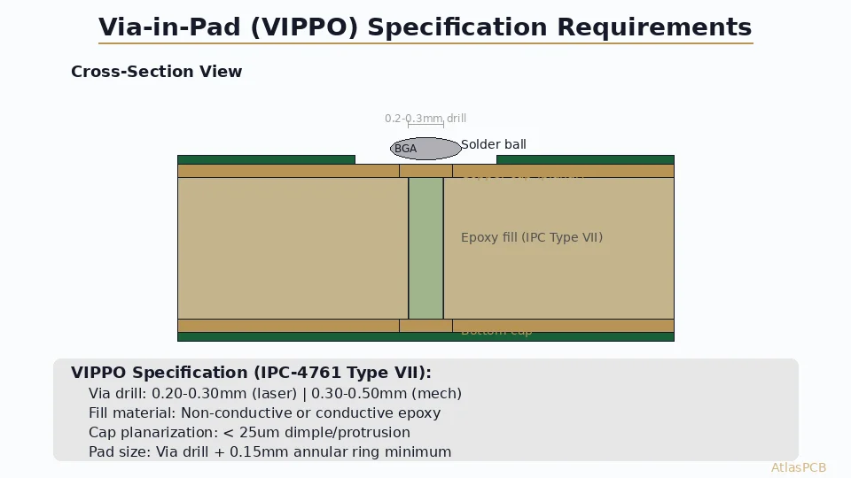
VIA-IN-PAD REQUIREMENTS (IPC-4761 Type VII):
- Applicable vias: All vias within BGA/LGA pad fields as marked on
  documentation layer [XX]
- Fill material: Non-conductive epoxy
- Planarization: Required prior to cap plating
- Cap plating: Minimum 25 µm copper over fill, both sides
- Maximum dimple: 25 µm (per IPC-6012 Class 2) [or 1 mil for Class 3]
- Maximum protrusion: 25 µm above surrounding copper
- Surface finish: [ENIG / ENEPIG / OSP] applied over cap plating
Why Via-in-Pad Specifications Fail at Fabrication
The most common reason via-in-pad boards get flagged during DFM review—or worse, built incorrectly—is incomplete or ambiguous fab notes. A fabricator who sees vias inside pads in your Gerber data but no explicit VIPPO callout faces a decision: assume you want filling (expensive, adds process steps) or assume it is a design error (flags for engineering query, delays your order by 24-48 hours).
The problem compounds because via-in-pad is not a single process. IPC-4761 defines seven distinct types of via protection, from simple tenting (Type I) through filled and capped (Type VII). When an engineer writes “fill all vias in BGA area” without referencing the IPC type, the fabricator must guess whether you mean just plugging (Type V/VI) or the full fill-planarize-cap sequence (Type VII). These processes have different costs, different reliability outcomes, and different dimensional tolerances.
A complete via-in-pad specification eliminates ambiguity by stating explicitly: which vias require treatment, what fill material to use, what dimple tolerance is acceptable, and whether cap plating is required. The fifteen minutes spent writing a proper fab note saves days of back-and-forth and prevents boards from arriving with incorrect via treatment.
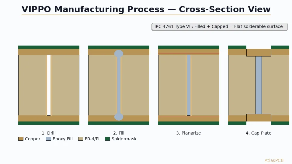
IPC-4761 Via Protection Types: Choosing the Right Level
The IPC-4761 standard defines a hierarchy of via protection methods. Understanding this hierarchy lets you specify exactly what you need without over-engineering (and overpaying) for via treatment on pads that do not require it.
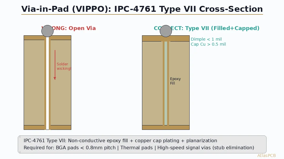
Type I (Tented) covers the via with solder mask. This is the standard treatment for vias NOT under component pads. The mask prevents solder from wicking into the via during reflow but provides no structural fill. Cost impact: zero (standard process).
Type V (Filled, not capped) plugs the via with epoxy but leaves the fill exposed. Suitable for vias that need to be plugged to prevent solder wicking but are not directly under component pads—for example, vias near (but not inside) fine-pitch pads where mask tenting alone might crack. Cost impact: moderate.
Type VII (Filled and capped - VIPPO) is the full process: fill with epoxy, planarize the surface flat, then plate copper over the fill to create a continuous pad surface. This is what you need for any via that sits directly under a BGA ball pad, QFN exposed pad, or any pad that receives solder paste. The cap plating creates a flat, solderable surface with controlled dimple that behaves identically to a standard SMD pad during assembly. Cost impact: significant (adds 2-3 process steps, increases lead time 2-3 days).
A common and costly mistake is specifying Type VII for ALL vias on a board when only the BGA field requires it. Your fab note should clearly delineate which vias get Type VII treatment (expensive) and which get standard Type I tenting (free). On a typical BGA-dense design, only 20-40% of total vias need VIPPO treatment. Specifying the full board adds unnecessary cost.
DFM REVIEW INCLUDED
We Verify Your Via-in-Pad Specs Before Production
Upload your design files. Our engineering team reviews VIPPO requirements against your BGA footprints and confirms process compatibility before quoting.
Upload Design Files ›Fill Material Selection: Conductive vs Non-Conductive Epoxy
The choice between conductive and non-conductive via fill is driven by thermal requirements, not electrical connectivity. Both types provide the mechanical function of supporting cap plating and preventing solder wicking. The difference lies in thermal conductivity and cost.
Non-conductive epoxy (standard, lower cost) has a thermal conductivity of approximately 0.5-0.8 W/mK. For signal vias under BGA pads—where the via carries data rather than dissipating power—this is entirely adequate. The via barrel copper provides the electrical connection regardless of fill material. Non-conductive fill is available from all quality PCB fabricators and adds minimal cost beyond the filling process itself.
Conductive epoxy (silver-filled, premium) achieves 3-5 W/mK thermal conductivity—roughly 5x better than non-conductive. This matters when vias serve as the primary thermal path from a high-power component to an internal copper plane or bottom-side heatsink. The classic application is thermal via arrays under QFN exposed pads or LED thermal pads. However, conductive fill costs 30-50% more than non-conductive, may require separate fill operations (if the board has both types), and has slightly higher CTE mismatch with surrounding laminate.
When to mix fill types on the same board: If your design has both BGA signal pads (non-conductive fill adequate) and a QFN thermal pad (conductive fill beneficial), you can specify different fill types by zone. However, some fabricators charge an additional setup fee for dual-fill processing. If the thermal via array is only 10-20 vias, the cost of conductive fill may exceed the thermal benefit compared to simply adding more non-conductive-filled vias to compensate with total copper barrel cross-section.
Dimple and Planarization Tolerances
After via filling and planarization, the surface will not be perfectly flat—there will be either a slight depression (dimple) or slight protrusion where the fill material shrinks or expands relative to the surrounding copper. Controlling this dimensional tolerance is critical for solder paste printing and BGA assembly yield.
IPC-6012 specifies maximum dimple depth of 25 microns for Class 2 and Class 3 boards. In practice, Class 3 assemblies for aerospace and medical often tighten this to 12-15 microns through internal workmanship standards. The reason is straightforward: a deeper dimple under a BGA pad creates a solder paste reservoir that produces inconsistent solder joint volume, leading to void formation or insufficient wetting on adjacent balls.
Your fab note should state the dimple tolerance explicitly rather than relying on the fabricator to assume a class level. If your assembly house has validated their process at 25 microns dimple, specify that. If they require tighter control, specify the tighter number and accept the yield impact (some vias will require rework or the cost of more aggressive planarization).
Protrusion is equally important. If the fill material protrudes above the pad surface, it creates an uneven stencil printing surface that can cause solder paste bridging or incomplete gasket seal. Specify maximum protrusion equal to or less than your dimple tolerance.
PRECISION MANUFACTURING
Dimple Control Within 15 Microns for Fine-Pitch BGA
Our VIPPO process achieves consistent dimple depth across via sizes from 0.10mm laser to 0.30mm mechanical drill. Validated for 0.4mm-pitch BGA assembly.
Request Capability Sheet ›Common Fab Note Mistakes That Delay Production
Mistake 1: “Fill all vias” — This is the most expensive three words in PCB fabrication. If your board has 5000 vias and only 800 are under BGA pads, you just tripled your via processing cost for no benefit. Always specify a zone, layer reference, or net class that identifies which vias require filling.
Mistake 2: No fill material specified — Some fab shops default to non-conductive epoxy, others have in-house conductive fill as standard. Without specification, you may get the wrong type or trigger an engineering query. State “non-conductive epoxy” or “conductive (silver-filled) epoxy” explicitly.
Mistake 3: Confusing via tenting with via filling — Solder mask tenting (covering a via with mask) and via filling (injecting epoxy into the barrel) are fundamentally different processes. Writing “plug all vias” when you mean “tent with mask” causes fabricators to quote filling operations at 3-5x the cost of simple tenting.
Mistake 4: No cap plating callout — If you need via-in-pad for BGA assembly but forget to specify cap plating, you may receive boards with filled-but-exposed vias (Type VI instead of Type VII). The exposed epoxy fill is not solderable, and your BGA pads will have reduced copper coverage that affects solder joint formation.
Mistake 5: Specifying VIPPO on blind/buried vias without noting it — Blind via filling is a different process than through-via filling (different fill heads, different cure schedules). If your HDI stackup has both through-vias and blind vias requiring VIPPO, list them separately with size ranges for each.
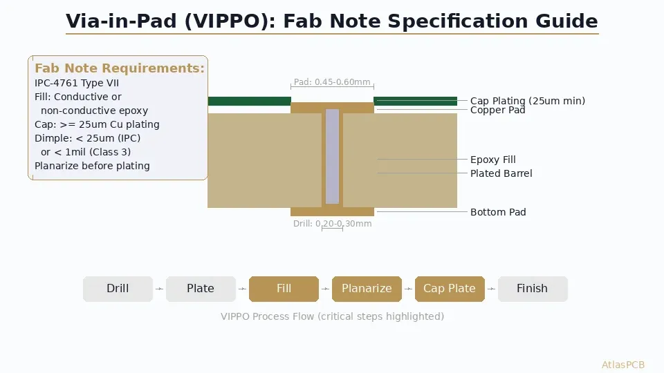
Complete Fab Note Example for a Complex Design
Here is a production-ready fab note for a 10-layer HDI board with multiple via types:
VIA TREATMENT SCHEDULE:

1. Through-vias under U1, U3 (BGA) pad fields:
   - IPC-4761 Type VII (filled and capped)
   - Drill: 0.25mm finished hole
   - Fill: Non-conductive epoxy
   - Cap plating: Min 25 µm copper, both sides
   - Dimple: Max 20 µm
   - Reference: Documentation layer 30

2. Blind vias Layer 1-2 (microvia):
   - IPC-4761 Type VII (filled and capped)
   - Laser drill: 0.10mm
   - Fill: Copper electroplate (stacked microvia)
   - Planarization required before next buildup

3. Thermal vias under U2 (QFN) exposed pad:
   - IPC-4761 Type VII (filled and capped)
   - Drill: 0.30mm finished hole
   - Fill: Conductive (silver-filled) epoxy
   - Cap plating: Min 25 µm copper
   - Reference: Documentation layer 30

4. All other through-vias:
   - IPC-4761 Type I (tented both sides with solder mask)
   - No filling required

ACCEPTANCE: Per IPC-6012 Class 3, IPC-A-600 Section 3.6
This level of detail eliminates 100% of ambiguity and ensures your fabricator prices and builds exactly what you designed.
ATLASPCB
Complex HDI with Via-in-Pad? We Build It Daily.
From 2-layer VIPPO to 5+N+5 HDI with stacked microvias. Upload your design and get a detailed quote with process confirmation.
Get HDI Quote ›Related Reading:
About AtlasPCB — We specialize in complex PCB manufacturing for HDI, RF, and high-reliability applications. Explore our HDI PCB manufacturing capabilities, free engineering DFM review, or get an full PCB manufacturing capabilities . Every order includes free engineering review. Get your quote.
Reviewed by AtlasPCB Engineering Team — IPC-certified manufacturing specialists with 15+ years of production experience in HDI, RF, and high-reliability PCB fabrication. Content based on factory floor data and real customer design reviews.
- via-in-pad
- VIPPO
- DFM
- fab notes
- IPC-4761
- BGA
- HDI
- PCB design rules