· AtlasPCB Engineering · Engineering · 6 min read
PCB Via Tenting vs Via Filling vs Via Plugging (VIPPO): When to Use Each Method
Complete guide to via protection methods in PCB manufacturing. Compare tenting, conductive/non-conductive filling, and VIPPO plugging for HDI, BGA, and high-reliability designs.

Why Via Protection Matters in Modern PCB Design
Every through-hole or microvia in a printed circuit board creates a potential reliability risk. Unfilled vias can trap flux residue, wick solder away from pads during reflow, or allow moisture ingress that leads to conductive anodic filament (CAF) growth. As board density increases and component pitches shrink below 0.5mm, choosing the right via protection method becomes a critical design decision.
The three primary approaches — tenting, filling, and plugging — represent a spectrum from cheapest/simplest to most expensive/capable. Understanding when each method is appropriate can save thousands of dollars on a production run or prevent field failures in safety-critical applications.
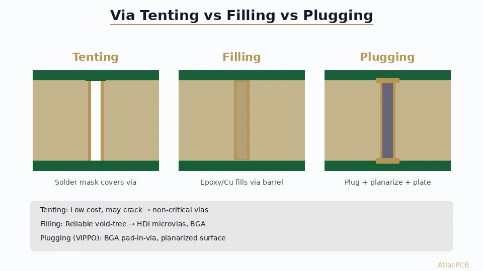
Via Tenting: The Low-Cost Default
Via tenting is the simplest and most economical via protection method. During the solder mask application process, liquid photoimageable (LPI) solder mask flows over the via opening, creating a thin membrane that covers the hole.
How Via Tenting Works
- Standard PTH or microvia is drilled and plated
- Solder mask is applied over the entire board surface
- The mask imaging step leaves the via covered (no opening defined)
- Mask bridges across the via opening, creating a tent
Tenting Limitations
The solder mask tent is typically only 15-25μm thick over the via center. This creates several reliability concerns:
- Tent cracking — thermal cycling can fracture the thin mask bridge
- Incomplete coverage — vias larger than 0.3mm diameter may not tent reliably
- Solder wicking — if the tent cracks during reflow, solder can flow into the via
- Not suitable for via-in-pad — no flat surface for component mounting
When to Specify Tenting
Via tenting is appropriate for:
- Non-critical signal vias away from component pads
- Prototype boards where cost minimization is priority
- Vias ≤ 0.3mm (12mil) diameter with mask on both sides
- Low-reliability consumer electronics (IPC Class 2)
Per IPC-4761 Type I, tenting requires solder mask coverage on one or both sides without any fill material.
Via Filling: Reliable Void-Free Protection
Via filling injects material — either non-conductive epoxy or conductive paste — into the via barrel, completely eliminating the hollow interior. This prevents solder wicking, improves thermal conductivity, and enables subsequent surface planarization.
Non-Conductive Epoxy Fill (IPC-4761 Type VI/VII)
Non-conductive epoxy fill is the most common filling method for standard HDI boards:
Process:
- Screen-print epoxy into via holes from one side
- Vacuum-assist to eliminate trapped air
- Cure at 150-170°C for 60-90 minutes
- Surface grinding to remove excess (planarization)
Properties:
- CTE: 40-60 ppm/°C (matched to FR-4)
- Tg: 150-170°C
- Dielectric constant: 3.5-4.0
- Thermal conductivity: 0.3-0.5 W/mK
Conductive Copper Fill
Conductive fill uses copper-particle-loaded paste for applications requiring thermal or electrical conductivity through the via:
- Thermal conductivity: 3-10 W/mK (vs 0.3 for epoxy)
- Electrical resistance: < 2mΩ per via
- Cost premium: 30-50% over non-conductive fill
- Applications: thermal vias under QFN/BGA, power distribution
Via Fill Quality Metrics
Per IPC-6012 Class 3, filled vias must meet:
- Fill depth: ≥ 80% of via depth (no dimple > 20% of board thickness)
- Void area: < 25% of via cross-section
- Planarization: ±10μm from copper surface after grinding
Need Precision Via Filling for Your HDI Design?
AtlasPCB delivers IPC Class 3 via fill with <2% void rate. Our laser-drilled microvias and VIPPO capability support the most demanding HDI stackups.
Get a Quote →Via Plugging (VIPPO): The Premium Solution for BGA Via-in-Pad
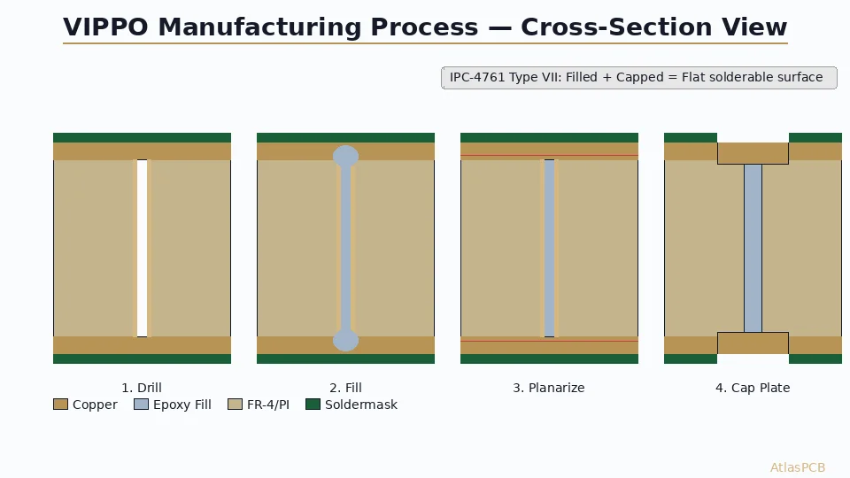
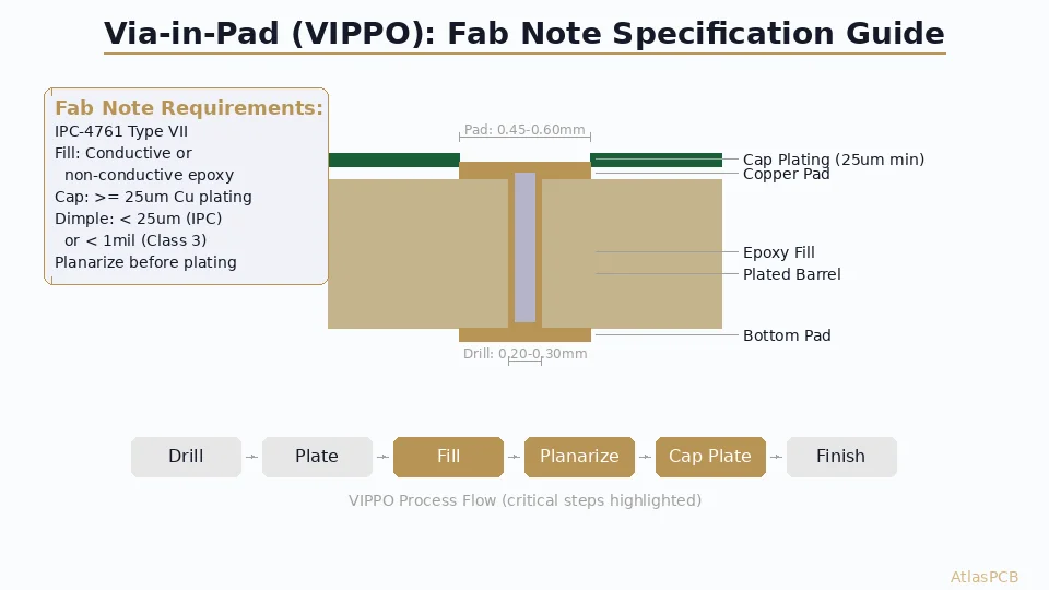
VIPPO — Via-In-Pad Plated Over — is the most advanced via protection method. It fills the via, planarizes the surface, then electroplates copper over the top to create a perfectly flat, solderable pad. This is essential for fine-pitch BGA designs where vias must be placed directly in component landing pads.
VIPPO Process Flow
- Drill — Laser drill microvias or mechanical drill through-holes
- Plate — Electroless + electrolytic copper plating of via barrel
- Fill — Non-conductive or conductive paste injection
- Cure — Thermal cure of fill material (150-170°C)
- Planarize — Ceramic belt grinding to remove fill excess
- Cap plate — Electroplate 20-30μm copper over the filled, flat surface
- Pattern — Standard photolithography defines pad geometry
Why VIPPO Is Essential for Modern BGA Design
With BGA pitches at 0.4mm and below, there isn’t sufficient routing space between pads to fan out all signal vias. Via-in-pad eliminates the need for fan-out traces by placing the via directly in the BGA landing pad.
Without VIPPO, via-in-pad designs suffer from:
- Solder wicking into unfilled vias during reflow
- Voiding in solder joints (reducing fatigue life by 30-50%)
- Uneven pad surfaces causing head-in-pillow defects
- Unreliable connections in automotive/aerospace applications
VIPPO Design Rules
| Parameter | Typical Value |
|---|---|
| Via diameter | 0.1-0.3mm |
| Pad diameter | Via + 0.15mm minimum |
| Cap plating thickness | 20-30μm |
| Surface flatness | ±15μm |
| Maximum aspect ratio | 0.8:1 (depth:diameter) for microvias |
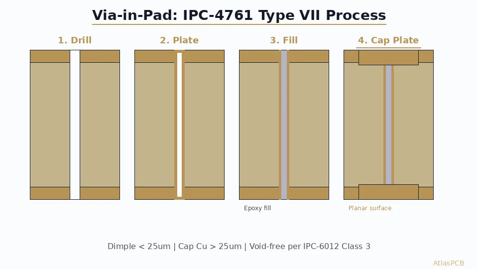
IPC-4761 Via Protection Classification
IPC-4761 defines seven types of via protection, providing a standardized specification language:
- Type I — Tented (mask covered, one side)
- Type II — Tented (mask covered, both sides)
- Type III — Plugged (mask plug, one side)
- Type IV — Plugged (mask plug, both sides)
- Type V — Filled (conductive or non-conductive)
- Type VI — Filled and capped (one side plated over)
- Type VII — Filled and capped (both sides plated over) — this is VIPPO
When specifying via protection on your fabrication drawing, reference the IPC-4761 type number for unambiguous communication with your manufacturer.
Cost Comparison and Decision Matrix
| Method | Added Cost/Via | Lead Time Impact | Best For |
|---|---|---|---|
| Tenting | $0.00 | None | Non-critical, ≤12mil vias |
| Epoxy Fill | $0.02-0.05 | +1-2 days | HDI microvias, thermal vias |
| Conductive Fill | $0.05-0.10 | +2-3 days | Power/thermal management |
| VIPPO | $0.08-0.15 | +3-5 days | BGA via-in-pad, any-layer HDI |
Decision Flowchart
- Is the via under a BGA or QFN pad? → VIPPO
- Does the via carry significant thermal load? → Conductive fill
- Is this an HDI microvia in a stacked structure? → Epoxy fill
- Is the via diameter ≤ 0.3mm and non-critical? → Tenting
- IPC Class 3 reliability required? → Fill (minimum)
Manufacturing Considerations
Aspect Ratio Limits for Via Filling
Via filling becomes increasingly difficult as aspect ratio increases:
- ≤ 1:1 — Standard fill process, high yield
- 1:1 to 1.5:1 — Requires vacuum-assisted fill
- > 1.5:1 — May require multiple fill cycles or special materials
For through-holes in boards > 2.0mm thick, consider back-drilling rather than filling to reduce aspect ratio challenges.
Common Fill Defects and Prevention
Dimpling — Depression in the fill surface after cure
- Cause: Insufficient fill volume or shrinkage during cure
- Prevention: Overfill by 10-15%, proper cure profile
Voiding — Trapped air bubbles within the fill
- Cause: Inadequate vacuum, fast fill speed
- Prevention: Vacuum < 5 torr, controlled injection rate
Delamination — Fill separating from via barrel wall
- Cause: Contamination, CTE mismatch
- Prevention: Proper desmear, CTE-matched fill material
Design Guidelines for Via Protection Specification
When creating your PCB fabrication notes, specify via protection clearly:
Via Fill Requirements:
- All blind/buried vias: IPC-4761 Type V (non-conductive fill)
- BGA via-in-pad locations: IPC-4761 Type VII (VIPPO)
- All other through-hole vias: IPC-4761 Type II (tented both sides)
- Maximum dimple depth: 75μm
- Maximum void area: 25% of via cross-section per IPC-6012 Class 3
Further Reading
- VIPPO Via-in-Pad Design and Manufacturing Guide
- HDI Microvia Stacked vs Staggered Reliability
- PCB Blind Via Fill Technology
- BGA Pad Design and Via-in-Pad Solder Voiding Prevention
Ready to specify via fill for your next design? AtlasPCB’s engineering team can review your stackup and recommend the optimal via protection strategy for your reliability class and budget. Request a free DFM review →
About AtlasPCB — We specialize in complex PCB manufacturing for HDI, RF, and high-reliability applications. Explore our HDI PCB manufacturing capabilities, or get an full PCB manufacturing capabilities . Every order includes free engineering review. Get your quote.
Reviewed by AtlasPCB Engineering Team — IPC-certified manufacturing specialists with 15+ years of production experience in HDI, RF, and high-reliability PCB fabrication. Content based on factory floor data and real customer design reviews.
- via filling
- via tenting
- VIPPO
- HDI PCB
- BGA design
- PCB manufacturing
- via plugging
- IPC-4761