· AtlasPCB Engineering · Engineering · 11 min read
PCB EMI Shielding: Via Fencing, Board-Level Shield Cans, and Grounding Strategies
Complete guide to PCB-level EMI shielding techniques including via fencing design rules, board-level shielding can selection, grounding strategies, and IPC/FCC compliance for mixed-signal and RF designs.
Introduction: Why EMI Shielding Matters at the PCB Level
Electromagnetic interference remains one of the top causes of product redesigns and regulatory compliance failures. According to industry data, approximately 50% of first-pass EMC test failures trace back to PCB-level radiation — not cable emissions or enclosure gaps. As operating frequencies push beyond 5 GHz for Wi-Fi 6E/7, 28 GHz for 5G mmWave, and 56+ Gbps for SerDes interfaces, effective board-level EMI containment has shifted from a “nice-to-have” to an absolute design requirement.
This guide covers the three primary PCB-level EMI shielding strategies — via fencing, board-level shield cans, and grounding architecture — with specific design rules, manufacturing constraints, and cost trade-offs that hardware engineers need for first-pass EMC success.
Understanding EMI Coupling Mechanisms on PCBs
Before selecting a shielding approach, engineers must identify the dominant coupling path:
Radiated coupling through substrate: High-speed digital signals and RF power amplifiers generate electromagnetic fields that propagate through the PCB dielectric. Without containment, these fields couple to adjacent sensitive circuits (LNAs, ADCs, crystal oscillators).
Surface wave propagation: At frequencies above 3 GHz, surface waves can travel along the PCB outer layers, coupling between distant circuits that share no direct trace connection.
Cavity resonance: In multilayer PCBs, the space between ground planes can resonate at specific frequencies, creating standing waves that amplify noise coupling.
Each mechanism requires a different mitigation approach — via fencing addresses lateral substrate coupling, shielding cans block vertical radiation, and proper grounding eliminates cavity resonance.
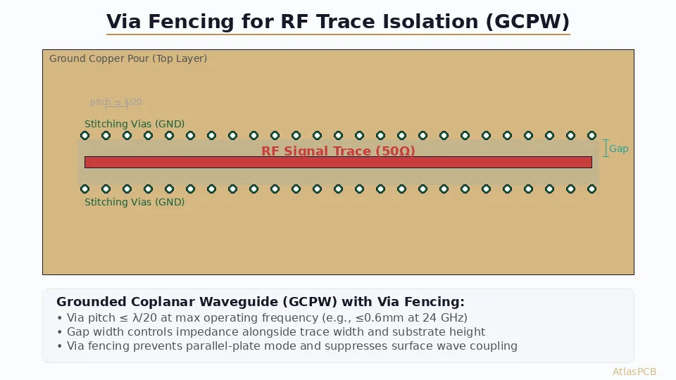
Via Fencing: Design Rules and Implementation
Operating Principle
A via fence creates an electromagnetic boundary by placing a continuous row of grounded vias between isolated circuit regions. When the via spacing is significantly smaller than the wavelength of the highest-frequency signal, the fence approximates a solid metal wall — a Faraday cage implemented within the PCB substrate.
Critical Design Parameters
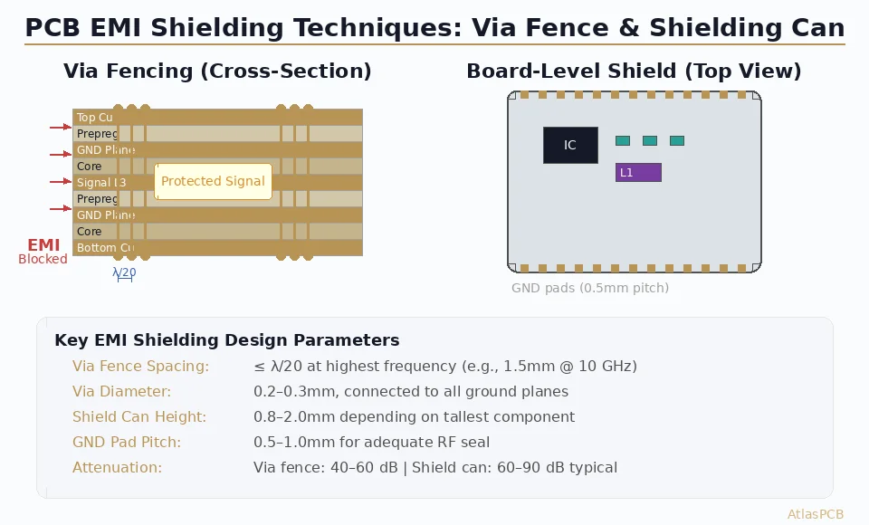
Via spacing (pitch): The fundamental rule is spacing ≤ λ/20 at the highest frequency of concern. This ensures that the gaps between vias are too small for electromagnetic waves to pass through efficiently.
| Frequency | Wavelength (FR-4, εr≈4.2) | Max Via Pitch (λ/20) | Recommended Pitch |
|---|---|---|---|
| 2.4 GHz | 61 mm | 3.0 mm | 2.0 mm |
| 5 GHz | 29 mm | 1.5 mm | 1.0 mm |
| 10 GHz | 15 mm | 0.75 mm | 0.5 mm |
| 28 GHz | 5.2 mm | 0.26 mm | 0.2 mm |
Via diameter: 0.2–0.3 mm (8–12 mil) finished hole size. Smaller vias allow tighter spacing but increase drilling cost. For frequencies above 10 GHz, consider laser-drilled microvias (0.1 mm) for achieving the required pitch.
Connection to ground planes: Every via in the fence must connect to ALL ground planes in the stackup. A via that misses even one ground layer creates a slot antenna effect that can actually worsen EMI at specific frequencies.
Fence continuity: The via fence must form a complete perimeter around the shielded region. Any gap larger than λ/20 acts as a slot radiator. Where signal traces must cross the fence boundary, route them on internal layers between two ground planes, and add extra vias on either side of the crossing point.
Implementation Best Practices
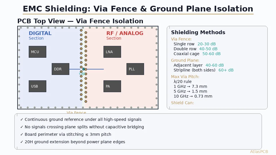
Double-row fencing: For applications requiring >50 dB isolation, use two parallel rows of vias offset by half the pitch. This staggered arrangement provides an additional 10–15 dB of attenuation compared to a single row.
Corner treatment: At fence corners, reduce the via pitch by 30% to compensate for the increased effective gap at bends. Place vias on both the inside and outside of the corner radius.
Integration with ground pour: The via fence should connect to a continuous ground copper pour on both the top and bottom layers. This copper pour serves as the “cap” of the Faraday cage, with the vias forming the walls.

Manufacturing Considerations
Via fencing adds minimal cost to standard PCB fabrication since the vias use the same drill sizes and plating processes as functional vias. The primary cost driver is board area — the fence perimeter plus keep-out zones can consume 5–15% of available routing space.
For HDI designs where drill hits are expensive, consider implementing the fence using [stacked microvias]/blog/hdi-microvia-stacked-vs-staggered-reliability/) connected across all layers rather than full-depth mechanical drills.
Board-Level Shielding Cans
When Via Fencing Isn’t Enough
Via fencing only blocks lateral propagation through the substrate. It cannot attenuate:
- Vertical radiation from components (ICs, inductors, crystals)
- Far-field emissions that exit the top surface of the PCB
- Near-field magnetic coupling from power inductors
Board-level shielding (BLS) cans address these limitations by enclosing the radiating or susceptible components in a stamped metal enclosure soldered directly to the PCB.
Shield Can Types
One-piece cans: Stamped from nickel-silver or tin-plated steel, these provide the highest shielding effectiveness (60–90 dB) but require the shield to be removed for rework — often damaging it in the process.
Two-piece (frame + lid): A permanent frame is soldered to the board, and a removable lid snaps or clips in place. Shielding effectiveness is 5–10 dB lower than one-piece (due to the lid-frame joint) but dramatically improves rework accessibility. This is the industry standard for volume production.
Fence + absorber: For ultra-high-frequency applications (>15 GHz), adding a thin layer of microwave absorber material inside the shield can prevents internal cavity resonance that would otherwise create shielding effectiveness notches at specific frequencies.
RF & MIXED-SIGNAL PCB MANUFACTURING
Need EMI-Compliant PCBs with Precision Via Fencing?
AtlasPCB manufactures complex multilayer boards with controlled-impedance ground planes, tight via pitch tolerances, and shield can landing pad accuracy — from prototype to production.
Request EMI-Optimized PCB Quote →PCB Design Requirements for Shield Cans
Ground pad ring: A continuous copper pad (0.5–1.0 mm width) must surround the shielded region on the component side. This pad connects to the internal ground plane through a row of vias spaced at ≤1.0 mm pitch — essentially combining via fencing with the shield can for maximum effectiveness.
Keep-out zones: Maintain 0.5 mm clearance between the shield can wall and the nearest component (1.0 mm for tall components that might interfere with the lid). The shield must clear the tallest enclosed component by at least 0.3 mm.
Ventilation and thermal considerations: Shield cans trap heat. For enclosed regions with >0.5W total power dissipation, add thermal vias beneath hot components connecting to internal or bottom-side ground planes for heat spreading. Some shield designs include perforated lids — though perforations larger than λ/20 compromise shielding.
Material Selection
| Material | SE @ 1 GHz | SE @ 10 GHz | Cost | Notes |
|---|---|---|---|---|
| Tin-plated steel | 80 dB | 70 dB | Low | Standard choice, magnetic shielding |
| Nickel-silver | 75 dB | 65 dB | Medium | Good corrosion resistance |
| Aluminum | 85 dB | 60 dB | Medium | Lightweight, needs solder coating |
| Mu-metal | 90+ dB | 55 dB | High | Low-frequency magnetic fields |
Grounding Strategies for EMI Control
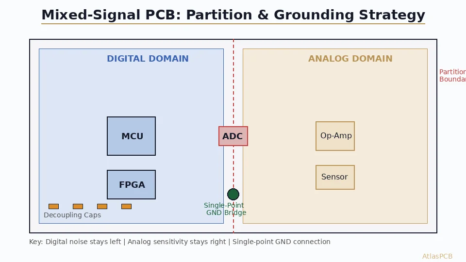
Split Ground vs Unified Ground
The traditional “split ground plane” approach — physically separating analog and digital ground regions — is increasingly recognized as problematic for modern mixed-signal designs. Current best practice uses a single, continuous ground plane with strategic placement to minimize coupling:
- Place sensitive analog circuits as far as possible from high-speed digital interfaces
- Route analog and digital signals in different layer pairs
- Use via fencing to create electromagnetic zones without splitting the ground plane
- Connect all ground regions at a single point near the power entry
Ground Plane Stitching
For multilayer PCBs, [ground plane stitching vias]/blog/pcb-ground-plane-stitching-via/) connect all ground layers together at regular intervals. For EMI-critical designs:
- Stitch every 5 mm in general areas
- Stitch every 2 mm around high-speed interfaces
- Stitch every λ/20 around RF sections (same rule as via fencing)
This prevents ground plane resonance and ensures consistent return current paths across the entire board.
Return Path Continuity
Every signal needs a return current path in the adjacent ground plane. EMI problems almost always trace back to return path discontinuities. Critical rules:
- Never route high-speed signals across ground plane splits or slots
- When changing signal layers, add [ground stitching vias]/blog/pcb-ground-plane-stitching-via/) within 1 mm of the signal via
- Keep decoupling capacitors within 2 mm of IC power pins with minimal loop area
- For differential pairs, maintain [symmetry in routing and reference planes]/blog/differential-pair-routing-rules-high-speed-serdes-pcb/)
Combining Techniques: Layered EMI Defense
The most effective EMI shielding uses multiple techniques simultaneously:
Layer 1 — PCB stackup: Start with a [properly designed stackup]/blog/controlled-impedance-pcb-stackup-design-rules/) that provides dedicated ground planes adjacent to every signal layer. This ensures return currents stay close to their signals.
Layer 2 — Via fencing: Divide the PCB into electromagnetic zones using via fences. Separate RF, high-speed digital, and sensitive analog sections.
Layer 3 — Board-level shields: Add metal shield cans over the most critical regions — typically the RF front-end, VCO/PLL, and sensitive ADC/DAC circuits.
Layer 4 — Component-level shielding: For individual noise sources (DC-DC converters, clock generators), use shielded component packages or ferrite bead filters at the boundary.
Design for Manufacturing: Via Fence and Shield Can Specifications
When documenting EMI shielding requirements for your PCB manufacturer, specify:
In the fabrication drawing:
- Via fence locations (copper layer marking)
- Via drill size and pitch (with tolerance: ±0.05 mm on pitch)
- Ground pad ring width and copper weight
- Minimum annular ring for fence vias
In the assembly drawing:
- Shield can part numbers and orientation
- Soldering method (reflow vs selective wave)
- Shield can placement sequence (usually last in reflow)
- Rework access requirements (removable lid, etc.)
IPC-2221B provides guidelines for board-level shielding implementation. IPC-6012 Class 3 requirements ensure the plating quality needed for reliable via fence performance.
Measurement and Validation
Pre-compliance Testing
Before sending boards for full EMC testing, validate shielding effectiveness using:
Near-field probing: Use H-field and E-field near-field probes to map radiation patterns on a bare board. Compare shielded vs. unshielded regions to verify isolation.
TDR impedance measurement: Verify that via fence and ground plane stitching haven’t created impedance discontinuities in critical signal paths. Request [impedance coupon testing]/blog/pcb-impedance-coupon-testing/) from your fabricator.
S-parameter measurement: For RF sections, measure isolation between ports on either side of a via fence using a VNA. Target ≥40 dB isolation at the operating frequency.
Simulation and Modeling Tools
Modern EMI design increasingly relies on electromagnetic simulation before fabrication:
3D Full-Wave Solvers (HFSS, CST): Model via fence effectiveness at specific frequencies. These tools can predict resonance frequencies of shielded cavities and identify optimal via placement. Computational cost is high, but results correlate well with measured shielding effectiveness.
2.5D Planar Solvers (Momentum, Sonnet): Faster than full 3D simulation, suitable for modeling via fence attenuation in planar PCB structures. Good for parametric sweeps of via spacing and diameter.
Rule-Based Design Checks: EDA tools (Altium, Cadence Allegro) include DRC rules for via fence spacing verification. Set up custom rules that flag any gap exceeding λ/20 at your maximum frequency.
Power Integrity Simulators (SIwave, ANSYS): Can identify ground plane resonance modes that create EMI vulnerabilities, guiding via stitching placement to suppress specific resonant frequencies.
The design iteration flow should be: (1) initial layout with via fencing per rules, (2) full-wave simulation to verify effectiveness, (3) adjust via placement to address any resonance or leakage issues, (4) prototype and validate with near-field scanning.
Common Design Mistakes
Even experienced designers make EMI-related errors. The most frequent:
Gap in the via fence at a connector exit: High-speed signals must cross the fence boundary to reach connectors. If the crossing point has inadequate via density, it becomes the dominant leakage path. Solution: create a dense via cluster (2× normal density) on both sides of every signal crossing point.
Ground plane cutout beneath a shield can: Routing signals under a shield often requires reference plane changes. If the plane is cut beneath the shield, the can’s effectiveness drops dramatically because the “floor” of the Faraday cage is compromised. Keep the ground plane completely continuous under all shielded regions.
Via fence connecting to only one ground layer: A via fence that connects to the top and bottom ground planes but not the middle ground planes provides shielding only for signals on those specific layers. For full-stackup isolation, every fence via must connect to every ground layer.
Resonant shield cavity: A shield can with no absorber material can resonate internally at frequencies where its dimensions equal λ/2. At resonance, the shield actually amplifies emissions rather than containing them. For shields larger than λ/4 in any dimension, include absorber material on the lid interior.
Cost Optimization
EMI shielding adds cost at multiple levels:
| Technique | Typical Cost Impact | Effectiveness |
|---|---|---|
| Via fencing (single row) | +2–5% board area | 40–50 dB |
| Via fencing (double row) | +5–10% board area | 50–65 dB |
| Shield can (one-piece) | +$0.15–0.50/unit | 60–90 dB |
| Shield can (two-piece) | +$0.30–1.00/unit | 55–80 dB |
| Additional ground planes | +1–2 layers | 20–30 dB per plane |
The most cost-effective approach is getting the [stackup design right]/blog/pcb-stackup-design-guide/) from the beginning. Adding ground planes early in the design process costs far less than adding shield cans after a failed EMC test.
Further Reading
- [EMC/EMI PCB Design Fundamentals]/blog/emc-emi-pcb-design/)
- [PCB Ground Plane Stitching Via Design]/blog/pcb-ground-plane-stitching-via/)
- [Controlled Impedance PCB Stackup Design]/blog/controlled-impedance-pcb-stackup-design-rules/)
- [Differential Pair Routing for High-Speed SerDes]/blog/differential-pair-routing-rules-high-speed-serdes-pcb/)
- [RF Microwave PCB Design Guidelines]/blog/rf-microwave-pcb-design/)
Ready to manufacture EMI-compliant PCBs? AtlasPCB provides engineering review for EMI-critical designs — including via fence spacing verification, ground plane continuity checks, and shield can pad optimization. Get a quote or explore our RF/high-speed PCB capabilities.
About AtlasPCB — We specialize in complex PCB manufacturing for HDI, RF, and high-reliability applications. Explore our RF and high-frequency PCB services, or get an impedance-controlled PCB manufacturing . Every order includes free engineering review. Get your quote.
Reviewed by AtlasPCB Engineering Team — IPC-certified manufacturing specialists with 15+ years of production experience in HDI, RF, and high-reliability PCB fabrication. Content based on factory floor data and real customer design reviews.
- emi shielding
- via fencing
- board-level shield
- rf pcb
- emc design
- grounding
- signal integrity