· AtlasPCB Engineering · Engineering · 9 min read
PCB Power Delivery Network Design for AI GPU Modules: VRM Layout, Copper Weight, and Decoupling Strategy
Engineering guide to designing PCBs that deliver 500-1000W to modern AI accelerator modules. Covers VRM placement strategy, copper weight selection for power planes, decoupling capacitor optimization, and thermal-aware PDN layout for GPU/TPU carrier boards.
The AI Power Challenge: Why Standard PCB Design Rules Break Down
Modern AI accelerator modules — Nvidia H100/B200, AMD MI300X, Google TPU v5 — consume 500-1000W in sustained workloads. This translates to 300-600 amperes of current delivered across multiple voltage rails, with transient slew rates exceeding 500A/microsecond during workload transitions. These power delivery requirements fundamentally exceed what conventional PCB design practices can handle.
To put this in perspective: a 700W GPU drawing 400A at 1.75V VCore needs a PDN impedance below 0.5 milliohms to maintain voltage within the 3% droop specification. Achieving that impedance target across the frequency range from DC to 100MHz requires simultaneous optimization of copper plane resistance, via inductance, and decoupling capacitor placement — each of which imposes constraints on every other aspect of the board design.
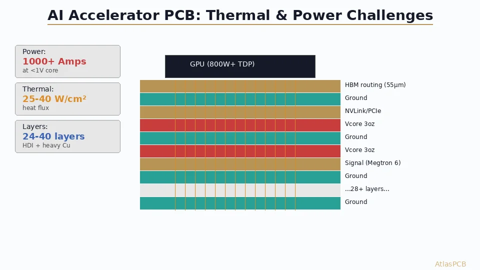
In our facility, we have seen AI hardware boards evolve from 12-layer designs (circa 2020 GPU cards) to 20-24 layer constructions for current-generation accelerators. The layer count increase is driven almost entirely by power delivery requirements — not signal routing density. Each additional power/ground pair reduces plane resistance and provides additional decoupling resonance points that flatten the impedance curve.
Stackup Architecture for AI GPU Carrier Boards
The stackup for a high-power AI accelerator PCB must balance three competing requirements: low-impedance power delivery, high-speed memory interface routing (HBM, GDDR7), and thermal management through the board structure.
A typical 20-layer stackup for a 700W-class GPU carrier board allocates layers as follows:
| Layer | Function | Copper Weight | Dielectric |
|---|---|---|---|
| L1 | Signal (component side) | 1oz | — |
| L2 | Ground (reference) | 2oz | Low-loss prepreg 3mil |
| L3 | Signal (HBM routing) | 1oz | Core 4mil |
| L4 | Ground (HBM reference) | 2oz | Prepreg 3mil |
| L5 | VCore power plane | 4oz | Core 3mil |
| L6 | Ground (PDN return) | 3oz | Prepreg 3mil |
| L7 | Signal (PCIe/NVLink) | 1oz | Core 4mil |
| L8 | Ground (reference) | 2oz | Prepreg 3mil |
| L9 | VRAM power plane | 3oz | Core 3mil |
| L10 | Ground (PDN return) | 3oz | Prepreg 3mil |
| L11 | Signal routing | 1oz | Core 4mil |
| L12 | Ground | 2oz | Prepreg 3mil |
| L13 | Aux power (1.8V, 3.3V) | 3oz | Core 3mil |
| L14 | Ground (PDN return) | 2oz | Prepreg 3mil |
| L15 | Signal routing | 1oz | Core 4mil |
| L16 | Ground (reference) | 2oz | Prepreg 3mil |
| L17 | Signal (memory channels) | 1oz | Core 4mil |
| L18 | Ground (reference) | 2oz | Prepreg 3mil |
| L19 | Signal (bottom routing) | 1oz | Prepreg 3mil |
| L20 | Signal (bottom component) | 1oz | — |
The critical design choice here is placing the VCore power plane (L5) and its return ground (L6) as adjacent layers with thin dielectric (3mil) between them. This tight coupling creates plane-pair decoupling capacitance of approximately 500pF per square inch — significant free decoupling that reduces the number of discrete capacitors needed.
At our facility, we process 4-5oz copper inner layers routinely for power electronics and AI hardware applications. The key manufacturing challenge is maintaining registration accuracy with thick copper layers — the copper weight creates uneven etching profiles that can shift feature positions by 1-2mil compared to standard 1oz layers. Our process compensates with tighter photolithography tolerances on heavy copper layers.
HIGH-POWER AI HARDWARE
Building an AI Accelerator Board? We Specialize in Heavy Copper Multi-Layer.
Up to 30 layers with 5oz inner copper, impedance-controlled signal layers, and thermal via arrays. Our engineers review your PDN stackup before production.
Upload Your Stackup ›VRM Placement Strategy: Distance Is Inductance
The single most impactful layout decision for AI GPU PDN performance is VRM-to-GPU distance. Every millimeter of PCB trace between the voltage regulator output and the GPU power pins adds parasitic inductance that directly limits transient response.
The physics is straightforward: a typical PCB power plane has inductance of approximately 0.3-0.5nH per millimeter of path length (depending on plane spacing and width). At 500A/us transient slew rate, each 1nH of loop inductance produces a voltage spike of 0.5mV — which sounds small until you consider that the total loop inductance budget for a 3% voltage droop specification at 400A might be only 5-10nH total.
Practical placement rules we apply for AI GPU boards:
Place multiphase VRM output inductors within 15-25mm of the GPU BGA package edge. This means the VRM controller IC is typically 30-40mm from the GPU (behind the inductors), with the output filter capacitors positioned between the inductors and the GPU.
Arrange output inductors in a semicircle or linear array along the nearest GPU edge rather than clustering them on one side. This distributes current injection points and reduces local current density in the power plane.
Position bulk capacitors (100-470uF) immediately adjacent to VRM output inductors for low-frequency bypass. Position mid-frequency capacitors (1-10uF) distributed between VRM and GPU. Position high-frequency capacitors (10-100nF) directly under or immediately adjacent to the GPU BGA.
In our DFM reviews for AI hardware customers, VRM placement violations are the most common critical issue we flag. Moving VRM components by even 10mm closer to the GPU often requires significant layout rework but can improve transient response by 20-30%. We recommend finalizing VRM placement before any signal routing begins.
Decoupling Strategy: Three Frequency Decades
Effective PDN design for AI accelerators requires distributed decoupling that covers the entire frequency range where the GPU generates supply noise. Modern GPUs have clock-gated compute blocks that switch on/off within nanoseconds, creating noise from 10kHz (workload variation) through 100MHz+ (clock harmonics).
No single capacitor type covers this range effectively. The solution is a three-tier decoupling architecture:
Tier 1: Bulk decoupling (10kHz - 1MHz) Capacitors: 100-470uF polymer aluminum or tantalum. Typically 6-12 pieces per power rail. Placement: near VRM output and distributed along power plane edges. Purpose: handle low-frequency load steps when GPU transitions between idle and full compute.
Tier 2: Mid-frequency decoupling (100kHz - 10MHz) Capacitors: 10-100uF X5R or X7R MLCC (0805 or 1206 package). Typically 40-80 pieces per power rail. Placement: distributed uniformly between VRM and GPU with 2-3mm spacing. Purpose: supply charge during transient events faster than VRM loop bandwidth (typically 50-200kHz).
Tier 3: High-frequency decoupling (1MHz - 100MHz) Capacitors: 10nF-1uF X7R MLCC (0201 or 0402 package). Typically 100-200+ pieces per power rail. Placement: directly under GPU BGA or within 3mm of power/ground ball positions. Purpose: suppress high-frequency resonances and supply instantaneous charge for clock-edge switching.
The capacitor count for a modern AI GPU board is staggering — often 400-600 decoupling capacitors total across all rails. This directly impacts PCB real estate and routing density. In our manufacturing, these boards require precise solder paste deposition on hundreds of 0201/0402 pads within tight proximity to the GPU BGA, demanding Class 3 assembly accuracy.
COMPLEX PDN FABRICATION
20+ Layer Boards with Heavy Copper PDN? We Build Them Daily.
3-5oz copper inner layers, 0.15mm laser vias for PDN stitching, and impedance control on signal layers — all in the same stackup. Tolerances verified on every panel.
Get Engineering Quote ›Via Stitching and Thermal Via Arrays for PDN
Power delivery via density is a critical but often underspecified parameter in AI GPU board design. Vias connecting power planes to component pads carry hundreds of amperes in aggregate, and their collective resistance and inductance directly impact PDN impedance.
For a GPU BGA with 200 power pins each carrying 2A average (400A total), the via resistance must be low enough that total via voltage drop stays below 10-20mV. A standard 0.3mm finished hole via with 25um copper plating has approximately 1.5-2 milliohms resistance. With 200 parallel vias, the aggregate via resistance is negligible — but only if all 200 vias are properly connected to unbroken power planes.
The challenge arises with signal vias that break through power planes, creating discontinuities that force current to route around via clearance holes. Dense via stitching between power and ground planes (independent of signal vias) provides alternative current paths and reduces the effective plane impedance.
Our standard recommendation for AI GPU carrier boards: minimum 1 power/ground stitching via per 4mm2 of plane area in the region between VRM and GPU. For the zone directly under the GPU BGA, increase to 1 via per 2mm2. These stitching vias should be 0.3mm or larger to minimize individual resistance.
From a manufacturing perspective, the high via density (often 8000-15000 vias per board) creates significant drilling time and cost. Boards in this category typically require 4-6 hours of drilling per panel compared to 30-60 minutes for a standard multilayer board. This is a significant cost driver that engineers should factor into their BOM estimates.
Thermal Management Integration with PDN Design
AI GPU boards generate 500-1000W of heat that must be conducted away from the GPU die through the board structure to heatsink mounting hardware. The PCB itself becomes a thermal management component — and the heavy copper planes used for power delivery also serve as thermal spreaders.
The 4-5oz power planes in the stackup provide excellent lateral thermal conductivity (approximately 400 W/m-K for copper versus 0.3 W/m-K for FR-4 dielectric). These planes spread heat from the GPU BGA footprint outward to the board edges where it can couple to chassis or heatsink mounting points.
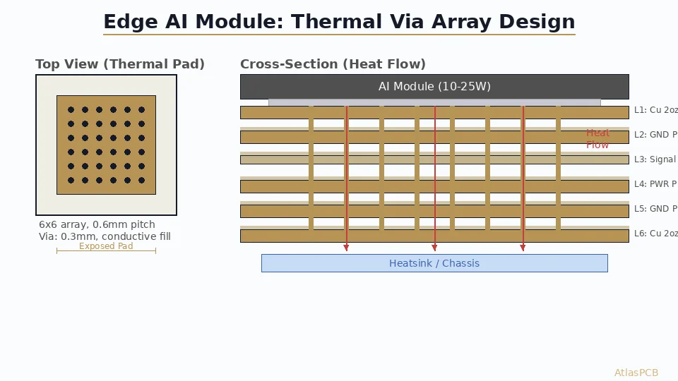
Thermal via arrays under the GPU thermal pad (typically a central exposed pad on the BGA package) provide vertical thermal conductivity through the board to the bottom-side heatsink. For a 1000W GPU, we recommend thermal via arrays with:
- Via diameter: 0.3-0.4mm (filled and capped for BGA assembly)
- Via pitch: 1.0-1.2mm center-to-center
- Via count: 100-200 in the thermal pad area
- Fill: Copper-filled (conductive) for maximum thermal conductivity
The interaction between thermal vias and power planes requires careful planning. Thermal vias that pass through all layers will break through every power and ground plane — creating exactly the discontinuities we want to avoid for PDN performance. The solution is to route thermal vias through dedicated ground planes (which can accommodate the antipad clearances without PDN impact) and avoid running them through the critical VCore power plane pair.
This thermal-versus-electrical tradeoff is one of the most complex aspects of AI GPU board design and represents an area where experienced layout teams earn their value. Getting it wrong means either inadequate thermal performance (GPU throttling) or compromised PDN integrity (voltage droop failures).
ATLASPCB
Designing AI Hardware? Let Our Engineers Review Your Stackup and PDN.
We fabricate 16-30 layer boards with 5oz copper power planes, filled thermal via arrays, and impedance-controlled high-speed layers. One partner from prototype to production.
Get Instant Quote ›Reviewed by AtlasPCB Engineering Team — 15+ years in advanced PCB fabrication for RF, HDI, and rigid-flex applications.
Related Reading:
About AtlasPCB — We specialize in complex PCB manufacturing for HDI, RF, and high-reliability applications. Explore our full PCB manufacturing capabilities, or get an instant online quote . Every order includes free engineering review. Get your quote.
Reviewed by AtlasPCB Engineering Team — IPC-certified manufacturing specialists with 15+ years of production experience in HDI, RF, and high-reliability PCB fabrication. Content based on factory floor data and real customer design reviews.
- AI PCB
- power delivery network
- VRM design
- GPU PCB
- high-current PCB