· AtlasPCB Engineering · Engineering · 17 min read
PTFE Substrate Handling & Fabrication: Challenges and Best Practices for RF PCBs
Master PTFE substrate fabrication for RF PCBs. Learn handling, drilling, lamination, and plating techniques to overcome Teflon's unique manufacturing challenges.
PTFE Substrate Handling & Fabrication: Challenges and Best Practices for RF PCBs
PTFE (polytetrafluoroethylene) — widely known by the trade name Teflon — is the substrate of choice for high-frequency RF and microwave PCB designs operating above 10 GHz. Its extraordinarily low dielectric loss, stable dielectric constant, and excellent thermal resistance make it indispensable for radar systems, satellite communications, 5G mmWave front-ends, and aerospace electronics.
But the same molecular properties that make PTFE electrically superior also make it one of the most difficult PCB substrates to fabricate. Its non-stick nature — the very reason Teflon coats frying pans — means it actively resists bonding with copper, adhesives, and plating chemistries. Its soft, waxy texture clogs drill bits and smears hole walls. Its high coefficient of thermal expansion creates dimensional instability during lamination and reflow.
If your design requires PTFE-based laminates, understanding these fabrication challenges — and the specialized techniques to overcome them — is the difference between a reliable product and a costly scrap pile. This guide covers every critical stage of PTFE substrate fabrication, from incoming material handling through final quality verification.
For a broader comparison of high-frequency substrate options, see our [RF PCB materials comparison guide]/blog/rf-pcb-materials-comparison/).
Understanding PTFE Material Properties
Before diving into fabrication techniques, it’s essential to understand why PTFE behaves so differently from standard FR-4 on the manufacturing floor. The properties that make PTFE electrically exceptional are the same ones that create fabrication headaches.
Electrical Properties
PTFE’s appeal in RF applications comes from its outstanding dielectric performance:
- Dielectric constant (Dk): 2.1–2.2 at 10 GHz (compared to 4.2–4.5 for FR-4)
- Loss tangent (Df): 0.0004–0.0009 at 10 GHz (compared to 0.018–0.025 for FR-4)
- Dk stability: Varies less than ±0.5% across the 1–40 GHz range
This combination of low Dk and ultra-low Df means signals propagate with minimal attenuation, making PTFE essential for applications where every fraction of a dB matters. For guidance on how dielectric properties influence substrate selection, consult our [high-frequency PCB substrate selection guide]/blog/high-frequency-pcb-substrate-selection-dk-df/).
Mechanical Properties — The Fabrication Challenge
The carbon-fluorine bonds that give PTFE its electrical superiority also create significant mechanical challenges:
| Property | PTFE Substrate | FR-4 | Fabrication Impact |
|---|---|---|---|
| Surface energy | 18–20 dynes/cm | 42–45 dynes/cm | Resists bonding and plating adhesion |
| CTE (Z-axis) | 70–100 ppm/°C | 50–70 ppm/°C | Dimensional instability, barrel cracking |
| CTE (X/Y-axis) | 15–25 ppm/°C | 14–17 ppm/°C | Registration challenges |
| Hardness | Very soft, waxy | Rigid, glass-reinforced | Drill smearing, routing difficulty |
| Moisture absorption | <0.02% | 0.10–0.20% | Minimal — one advantage |
| Tg | 327°C (melting, no Tg) | 130–180°C | Different thermal behavior |
The surface energy difference is the root cause of most PTFE fabrication problems. At 18–20 dynes/cm, PTFE has one of the lowest surface energies of any solid material. For context, effective bonding typically requires surface energy above 40 dynes/cm. This means PTFE in its natural state will not reliably bond to copper foil, adhesive prepregs, or plating chemistries without aggressive surface modification.
Common PTFE Laminate Systems
The most widely used PTFE-based laminate families in RF PCB manufacturing include:
- Ceramic-filled PTFE: Dk 2.9–10.2, reinforced with ceramic powder for CTE improvement and mechanical stability. Widely used for patch antennas and filters.
- Glass microfiber-reinforced PTFE: Dk 2.2–2.5, woven or random glass microfiber for dimensional stability. The workhorse for low-loss microstrip and stripline designs.
- PTFE/hydrocarbon blends: Modified PTFE systems with improved processability while retaining most of the electrical performance. These bridge the gap between pure PTFE and thermoset systems.
Each system has slightly different fabrication requirements, but the core challenges — adhesion, drilling, and CTE management — apply across all PTFE substrates.
Handling and Storage Requirements
PTFE substrates demand more careful handling than FR-4 from the moment they arrive in the fabrication facility. Contamination that would be inconsequential on FR-4 can cause catastrophic adhesion failures on PTFE.
Storage Conditions
- Temperature: Store at 18–25°C (64–77°F) in a climate-controlled environment
- Humidity: Maintain 40–60% RH — while PTFE itself doesn’t absorb moisture, associated adhesive layers and copper foil do
- Orientation: Store flat on clean shelves. PTFE’s soft nature means stacking heavy panels can cause permanent deformation
- Shelf life: Use within 12 months of manufacture for optimal bonding performance; track lot dates rigorously
Contamination Prevention
PTFE’s low surface energy means any surface contamination — fingerprints, dust, oils, or particulates — will have an outsized effect on adhesion and plating quality:
- Always wear clean, lint-free gloves when handling PTFE panels. Natural skin oils are virtually impossible to remove from PTFE surfaces using standard cleaning
- Clean panels before processing with isopropyl alcohol (IPA) wipe-down, followed by a deionized water rinse
- Never use marker pens or adhesive labels directly on PTFE surfaces — residues can interfere with surface treatment chemistry
- Separate PTFE work from FR-4 production lines where possible. FR-4 drilling dust is abrasive and can embed in soft PTFE surfaces
Pre-Processing Bake
Although PTFE absorbs almost no moisture, a pre-processing bake is still recommended:
- Temperature: 120–150°C for 2–4 hours
- Purpose: Remove any trapped volatiles from the adhesive system and copper-clad interface, not the PTFE itself
- Timing: Bake immediately before lamination or surface treatment — don’t let baked panels sit in open shop conditions for more than 4 hours
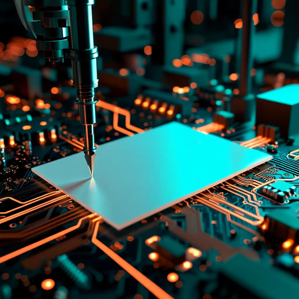
Drilling Challenges and Solutions
Drilling is arguably the most problematic fabrication step for PTFE substrates. The material’s soft, waxy consistency causes problems that simply don’t occur with rigid FR-4.
Why PTFE Is Difficult to Drill
When a drill bit enters PTFE material, several problems emerge simultaneously:
Smearing: PTFE doesn’t chip cleanly like glass-reinforced epoxy. Instead, it smears and flows around the drill bit, leaving a film of melted PTFE coating the hole wall. This smear layer prevents subsequent plating chemistry from reaching the copper inner layers.
Delamination: The weak bond between PTFE and copper (even with treated foil) means aggressive drill entry can lift the copper from the substrate at the hole perimeter.
Hole wall roughness: PTFE tends to tear rather than cut cleanly, producing inconsistent hole wall quality that degrades plating adhesion and via reliability.
Bit loading: PTFE debris wraps around drill flutes rather than ejecting as chips, reducing cutting efficiency and generating heat.
Optimized Drilling Parameters
Successful PTFE drilling requires significant parameter adjustments compared to FR-4:
| Parameter | FR-4 Typical | PTFE Optimized | Notes |
|---|---|---|---|
| Spindle speed | 80,000–120,000 RPM | 40,000–60,000 RPM | Reduced to prevent melting |
| Infeed rate | 2.0–3.0 m/min | 0.8–1.5 m/min | Slower for cleaner cutting |
| Retraction rate | 15–25 m/min | 10–15 m/min | Controlled to prevent tear-out |
| Hit count per bit | 2,000–3,000 | 500–1,000 | Frequent changes essential |
| Chip load | 0.025–0.05 mm/rev | 0.02–0.03 mm/rev | Finer chip load for PTFE |
| Stack height | 3–4 panels | 1–2 panels | Reduced stack for precision |
Drill Bit Selection
Standard FR-4 drill bits are poorly suited for PTFE. Use bits specifically designed for soft substrates:
- Geometry: Low-angle point geometry (115–118° included angle) with polished flutes to prevent PTFE adhesion
- Material: Solid carbide with diamond-like carbon (DLC) coating significantly reduces PTFE sticking
- Flute design: Deep, open flutes with aggressive helical angles aid chip evacuation from the soft material
- Undercut design: Slight negative rake angle helps shear PTFE cleanly rather than pushing it aside
Desmear for PTFE
Standard permanganate desmear used for FR-4 is ineffective on PTFE — the chemistry simply doesn’t attack the fluoropolymer. Instead, PTFE desmear requires:
- Plasma desmear: Oxygen/CF₄ gas plasma at 200–400W effectively removes PTFE smear from hole walls. This is the most common approach and produces excellent results. Process time: 15–30 minutes depending on smear severity.
- Sodium naphthalenide dip (hole wall only): A controlled short-duration exposure can remove smear while simultaneously preparing the hole wall surface for plating.
Plasma desmear is strongly preferred because it provides uniform treatment of all hole walls simultaneously and doesn’t introduce chemical contamination.
Surface Preparation Techniques for Adhesion
Surface preparation is the single most critical step in PTFE PCB fabrication. Without proper treatment, copper adhesion, plating adhesion, and interlayer bonding will fail — often not during manufacturing, but during thermal cycling in the field, which is far worse.
Sodium Naphthalenide (Na-Naph) Etching
Sodium naphthalenide etching is the gold standard for PTFE surface treatment and has been used successfully for over 40 years:
How it works:
- A solution of sodium metal dissolved in naphthalene/tetrahydrofuran is applied to the PTFE surface
- The sodium strips fluorine atoms from the PTFE polymer chain, replacing C-F bonds with C=C double bonds
- This creates a dark brown/black carbonized surface layer approximately 0.1–1.0 μm thick
- The carbonized layer has dramatically higher surface energy (≥45 dynes/cm) and bonds readily with copper and adhesives
Process parameters:
- Concentration: Typically 1.0–3.0 molar sodium in naphthalene/THF
- Temperature: Room temperature (20–25°C)
- Immersion time: 15–60 seconds (critical — over-etching weakens the surface layer)
- Rinse: Immediate thorough rinse in IPA followed by deionized water
- Shelf life after treatment: Process within 24–48 hours. The treated surface degrades with time and environmental exposure
Advantages:
- Proven reliability over decades of production use
- Excellent bond strength (typically 6–8 lb/in peel strength with rolled copper foil)
- Works on all PTFE formulations
Disadvantages:
- Toxic and flammable chemistry requiring careful handling
- Hazardous waste disposal requirements
- The treated surface discolors to dark brown/black — cosmetically unacceptable in some applications
- Batch-to-batch consistency requires tight process control
Plasma Treatment
Plasma treatment is an increasingly popular alternative that avoids the chemical hazards of sodium etching:
How it works:
- PTFE panels are placed in a vacuum chamber
- Gas plasma (typically O₂, Ar, or mixed O₂/Ar/CF₄) is generated at 100–500W RF power
- Energetic ions and radicals bombard the PTFE surface, breaking C-F bonds and introducing oxygen-containing functional groups (–OH, –COOH, –C=O)
- Surface roughness increases at the nanoscale, improving mechanical interlocking
Process parameters:
- Gas composition: O₂/Ar mix (70/30) is common; adding 5–10% CF₄ enhances etch uniformity
- Power: 200–400W RF
- Pressure: 200–500 mTorr
- Duration: 5–15 minutes
- Surface energy achieved: 40–55 dynes/cm (varies with parameters)
Advantages:
- No chemical waste — dry process
- Uniform treatment across large panel areas
- No surface discoloration
- Can treat hole walls and surfaces simultaneously (dual-purpose with desmear)
- Environmentally friendly
Disadvantages:
- Capital equipment cost (plasma chambers are expensive)
- Surface treatment decays faster than sodium etch — process within 8–24 hours
- Bond strength typically 10–20% lower than optimized sodium etch
- Requires careful parameter optimization for each PTFE formulation
Surface Treatment Selection Guidelines
| Criteria | Sodium Etch | Plasma | Recommendation |
|---|---|---|---|
| Bond strength (primary concern) | ✅ Superior | ⚠️ Good | Sodium etch |
| Environmental compliance | ⚠️ Hazardous waste | ✅ Clean | Plasma |
| Throughput | ⚠️ Batch dip | ✅ Large panels | Plasma |
| Cost per panel | ✅ Low chemical cost | ⚠️ High capital | Depends on volume |
| Hole wall + surface combo | ❌ Separate steps | ✅ Simultaneous | Plasma |
For most production environments, plasma treatment is becoming the preferred method due to environmental regulations and process integration advantages. However, for the highest reliability applications (aerospace, defense), sodium naphthalenide etching remains the benchmark.
Lamination and Bonding
Laminating PTFE layers — either to other PTFE layers or to FR-4 in hybrid constructions — requires specialized bonding materials and modified press cycles. Standard FR-4 prepregs cannot bond to PTFE even after surface treatment.
Bonding Materials for PTFE Lamination
Several bonding film and prepreg options exist for PTFE lamination:
- PTFE-based bondply: Thin PTFE films with adhesive treatment on both sides. Provides the best electrical match but requires high lamination temperatures (280–320°C).
- Thermoset bondply (e.g., FEP films): Fluorinated ethylene propylene copolymer films that bond at 290–310°C. Good dielectric properties (Dk ~2.1) with strong PTFE-to-PTFE adhesion.
- Modified acrylic adhesive films: Lower temperature bonding (160–180°C) but higher dielectric loss. Suitable for non-critical interlayer bonds.
- Low-flow FR-4 prepregs: For hybrid stackups where the prepreg bonds PTFE to FR-4 cores. Requires surface-treated PTFE.
Lamination Parameters
PTFE lamination differs significantly from FR-4 processing:
| Parameter | FR-4 Standard | PTFE-to-PTFE | PTFE/FR-4 Hybrid |
|---|---|---|---|
| Peak temperature | 175–185°C | 290–370°C* | 220–260°C |
| Ramp rate | 2–4°C/min | 2–3°C/min | 1.5–2.5°C/min |
| Pressure | 250–350 PSI | 100–200 PSI | 150–300 PSI |
| Dwell time at peak | 60–90 min | 15–30 min | 30–60 min |
| Cool-down rate | 2–3°C/min | 1–2°C/min | 1–2°C/min |
*Temperature depends on bonding system used
Critical Lamination Considerations
Pressure control is critical. Unlike FR-4 where higher pressure generally improves bond quality, excessive pressure on PTFE can cause:
- Resin squeeze-out from the bonding layer
- Dimensional distortion of the soft PTFE core
- Copper trace deformation on inner layers
- Thickness variation across the panel
Temperature ramp rate matters. Too-rapid heating creates thermal gradients that cause internal stress, warpage, and delamination. PTFE’s high CTE amplifies this effect — a 100 ppm/°C Z-axis CTE means a 0.030″ PTFE core expands by 0.0009″ over a 300°C lamination cycle. That expansion must be accommodated smoothly.
Cool-down is as important as heat-up. Rapid cooling locks in thermal stress. A controlled cool-down at 1–2°C/min allows the PTFE and bonding layers to relieve stress gradually, significantly improving long-term reliability.
Plating Challenges on PTFE
Electroless copper plating on PTFE hole walls and surfaces presents unique challenges directly related to the material’s low surface energy and chemical inertness.
Why Standard Plating Fails on PTFE
The standard electroless copper plating process for FR-4 follows this sequence: cleaner → conditioner → micro-etch → catalyst (Pd/Sn) → accelerator → electroless copper. On PTFE, this process fails because:
- Catalyst adhesion: Palladium-tin colloidal catalyst doesn’t adhere to untreated PTFE — it simply washes off during the rinse steps
- Wetting: Plating solutions bead up on PTFE surfaces rather than forming a uniform film
- Electroless copper adhesion: Even where copper nucleates, it has negligible adhesion to the PTFE surface
PTFE Plating Process Modifications
Successful plating on PTFE requires these additional/modified steps:
1. Surface treatment first — Sodium etch or plasma treatment (as described above) is mandatory before any plating process. This is non-negotiable.
2. Modified catalyst chemistry:
- Use high-activity colloidal Pd/Sn catalyst specifically formulated for low-surface-energy substrates
- Extended catalyst immersion time (5–8 minutes vs. 2–3 for FR-4)
- Double catalyst application (catalyst → rinse → catalyst) improves coverage uniformity
3. Specialized conditioning:
- Cationic surfactant conditioners designed for fluoropolymer surfaces
- These conditioners deposit a thin cationic film on the treated PTFE surface that promotes catalyst adsorption
4. Electroless copper bath modifications:
- Formaldehyde-based baths: Use higher formaldehyde concentration for faster nucleation
- Maintain bath temperature at the upper end of the operating range to improve wetting
- Extended plating time to build a minimum 25–35 μin (0.6–0.9 μm) electroless copper layer for reliable subsequent electroplating
5. Adhesion verification:
- Tape test (ASTM D3359) every lot — not optional
- Thermal stress test (288°C solder float for 10 seconds) to verify plating survives assembly temperatures
- Target peel strength: ≥4 lb/in for Class 2, ≥6 lb/in for Class 3 applications
Hybrid PTFE/FR-4 Stackup Considerations
Many RF designs don’t require PTFE on every layer. Hybrid stackups using PTFE for RF signal layers and FR-4 for digital, power, and ground layers offer significant cost savings while maintaining RF performance where it matters. For a detailed exploration of this approach, see our guide on [hybrid PCB stackups with Rogers and FR-4]/blog/pcb-hybrid-stackup-rogers-fr4/).
Why Go Hybrid?
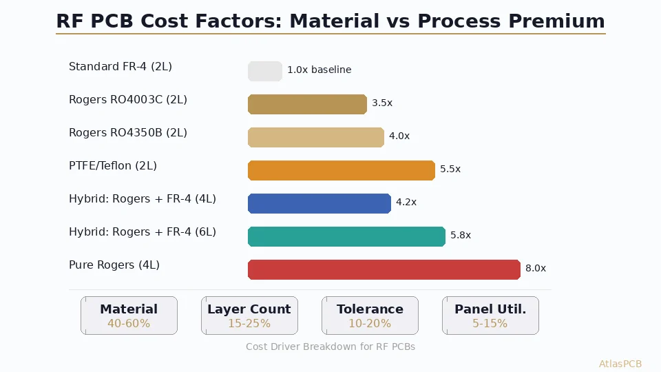
- Cost reduction: PTFE materials cost 10–20× more than FR-4. If only 2 of 8 layers need PTFE, the savings are dramatic
- Mechanical advantage: FR-4’s rigid glass-reinforced structure provides better board-level stiffness than an all-PTFE construction
- Process simplification: FR-4 layers can be processed using standard fabrication techniques; only the PTFE layers require specialized handling
- Component compatibility: Standard FR-4 solder mask and surface finishes can be applied to non-PTFE layers without modification
Typical Hybrid Stackup Configurations
A common 6-layer hybrid configuration for a 24 GHz automotive radar module:
Layer 1 (Top):    Copper — RF antenna patches
                  PTFE core (0.010″, Dk 2.2)
Layer 2:          Copper — Ground plane
- - - - - - - -  Bonding film (modified prepreg)
Layer 3:          Copper — Digital signals
                  FR-4 core (0.020″)
Layer 4:          Copper — Power plane
- - - - - - - -  Bonding film (modified prepreg)
Layer 5:          Copper — Ground plane
                  PTFE core (0.010″, Dk 2.2)
Layer 6 (Bottom): Copper — RF feed network
This configuration places PTFE on the outer RF layers where microstrip performance is critical, while the FR-4 interior handles non-RF functions. The symmetrical PTFE placement (top and bottom) helps manage warpage from CTE mismatch.
CTE Management in Hybrid Stackups
The CTE mismatch between PTFE and FR-4 is the primary reliability concern in hybrid designs:
- Z-axis CTE: PTFE (70–100 ppm/°C) vs. FR-4 (50–70 ppm/°C below Tg, 250+ ppm/°C above Tg)
- X/Y-axis CTE: PTFE (15–25 ppm/°C) vs. FR-4 (14–17 ppm/°C) — much closer match
Strategies for managing CTE mismatch:
- Symmetrical stackup design — Mirror PTFE and FR-4 layers about the center to balance thermal stress
- Ceramic-filled PTFE selection — Ceramic fillers reduce PTFE’s Z-axis CTE from 70–100 ppm/°C to 24–48 ppm/°C, much closer to FR-4
- Controlled via aspect ratios — Keep via aspect ratios ≤8:1 to prevent barrel cracking from Z-axis expansion
- Annular ring oversizing — Use minimum 5 mil annular rings (vs. 3.5 mil for FR-4-only) to accommodate registration variation from CTE differences
For more about managing material interactions in complex stackups, read our [PCB material selection guide]/blog/pcb-material-selection-guide/).
Sequential Lamination for Hybrid Boards
Hybrid PTFE/FR-4 boards typically require sequential lamination rather than a single press cycle:
Step 1: Laminate the FR-4 core layers using standard parameters (175–185°C)
Step 2: Image and etch inner layer patterns on the FR-4 subassembly
Step 3: Bond PTFE layers to the FR-4 subassembly using appropriate bonding film, with a second press cycle at the temperature required by the PTFE bonding system (220–260°C)
Step 4: Proceed with drilling and surface processing
This sequential approach prevents exposing FR-4 layers to temperatures above their Tg during the PTFE bonding step. Some advanced fabricators use specialized low-temperature PTFE bonding films that process at 185–200°C, enabling single-cycle lamination — but these are not universally available.
Routing and Mechanical Processing
Routing and scoring PTFE panels requires the same careful parameter adjustment as drilling:
- Router bit speed: 24,000–35,000 RPM (lower than FR-4’s typical 40,000–55,000 RPM)
- Feed rate: 30–50 inches/min (vs. 60–100 for FR-4)
- Bit type: Diamond-grit or carbide with DLC coating to prevent PTFE adhesion
- Depth-controlled routing: PTFE’s softness makes consistent depth control difficult. Use vacuum hold-down and rigid backer materials
- Tab routing: PTFE panels require wider tabs (≥0.080″) than FR-4 to prevent breakout during depanelization
V-scoring PTFE is generally not recommended. The soft material tears rather than fractures cleanly along the score line, producing ragged edges and potential delamination at the copper-PTFE interface.
Quality Control and Inspection
PTFE fabrication demands tighter process control and more frequent inspection points than standard FR-4 production:
In-Process Inspections
- Surface treatment verification: Contact angle measurement using deionized water. Untreated PTFE shows contact angles >108°; properly treated surfaces should measure <65° (sodium etch) or <75° (plasma). Measure within 1 hour of treatment.
- Drill quality: Cross-section every new drill parameter setup. Look for smear, delamination, and hole wall roughness. Automated optical inspection (AOI) of hole quality at higher frequency than FR-4 production.
- Lamination verification: Cross-section bond lines after each press run. Measure bondline thickness variation (target <10% across the panel). Check for voids and delamination using C-SAM (acoustic microscopy).
- Plating adhesion: Tape test per ASTM D3359 on every lot. Thermal stress test (solder float at 288°C × 10 seconds) on sample coupons.
Final Inspection Focus Areas
- Impedance testing: PTFE’s tight Dk tolerance (typically ±0.04) means impedance should be well controlled — but verify. TDR testing on every panel for RF-critical designs.
- Copper peel strength: Measure per IPC-TM-650, Method 2.4.8. Minimum 4 lb/in for general commercial, 6 lb/in for high-reliability.
- Microsection analysis: Evaluate plated through-hole integrity, paying special attention to the PTFE-copper interface at hole walls.
- Dimensional stability: Measure registration accuracy — PTFE’s higher CTE means tighter incoming tolerances may shift during processing.
Best Practices Summary
After years of production experience with PTFE substrates, these best practices consistently separate successful fabrication from problematic runs:
Treat surface preparation as the most critical process step. Bond failures are the number-one cause of PTFE PCB field returns. Invest in process control for sodium etch or plasma treatment.
Reduce drilling speeds by 40–50% from FR-4 parameters and change bits 3× more frequently. The cost of new carbide bits is negligible compared to scrapped panels.
Control lamination ramp rates and cool-down. Rapid thermal cycles create stress that manifests as delamination weeks or months later.
Process surface-treated PTFE within hours, not days. Surface treatment decay is real. Build production schedules around the treatment-to-next-step window.
Use ceramic-filled PTFE grades for hybrid stackups to minimize CTE mismatch with FR-4 layers.
Cross-section aggressively during process development. You cannot visually inspect bond quality, plating adhesion, or drill wall condition. Microsection analysis is the only way to validate process parameters.
Work with an experienced RF PCB fabricator. PTFE fabrication requires capital equipment (plasma chambers, specialized drills, controlled lamination presses) and trained operators that general-purpose shops may not have. See our overview of [RF PCB manufacturer capabilities]/blog/rf-pcb-manufacturer/).
Conclusion: Partner with PTFE Fabrication Experts
PTFE substrates unlock performance levels that no other PCB material can match at microwave and millimeter-wave frequencies. But realizing that performance in a manufactured board requires fabrication expertise that goes far beyond standard PCB processing.
Every stage — from storage and handling through drilling, surface treatment, lamination, plating, and routing — demands specialized knowledge and equipment. The margin for error is slim, and failures often don’t appear until thermal cycling in the field.
At Atlas PCB, we’ve invested in the equipment, processes, and engineering expertise to handle PTFE substrates reliably at production volumes. Whether you need pure PTFE multilayer construction or cost-optimized [hybrid stackups]/blog/pcb-hybrid-stackup-rogers-fr4/), our engineering team can help you navigate the fabrication challenges and deliver boards that perform as designed.
For comprehensive guidance on selecting the right material system for your frequency range, explore our [RF microwave PCB design resource]/blog/rf-microwave-pcb-design/) or review our [RF PCB design guidelines]/blog/rf-pcb-design-guidelines/).
Ready to discuss your PTFE PCB project? Our RF fabrication engineers are available to review your design and recommend the optimal fabrication approach.
Further Reading
- [Rogers PCB Fabrication: Material Sourcing, Lead Times & Quality Control]/blog/rogers-pcb-fabrication/)
- [ENEPIG vs ENIG: Which PCB Surface Finish for Your Design?]/blog/enepig-vs-enig/)
- [PCB Surface Finish Selection — ENIG vs HASL vs OSP vs Hard Gold vs ENEPIG]/blog/pcb-surface-finish-enig-hasl-osp-hard-gold-enepig/)
- [mmWave PCB Material Selection: Rogers vs Megtron vs LCP for 5G and 6G Applications]/blog/mmwave-pcb-material-selection-rogers-megtron-lcp-5g-6g/)
- [HDI PCB Design for 5G Antenna Integration: Signal Integrity Challenges in Millimeter-Wave Applications]/blog/hdi-5g-antenna-integration-pcb-design/)
- High-Frequency RF PCB Services
About AtlasPCB — We specialize in complex PCB manufacturing for HDI, RF, and high-reliability applications. Explore our RF and high-frequency PCB services . Every order includes free engineering review. Get your quote.
Reviewed by AtlasPCB Engineering Team — IPC-certified manufacturing specialists with 15+ years of production experience in HDI, RF, and high-reliability PCB fabrication. Content based on factory floor data and real customer design reviews.
- PTFE
- RF PCB
- substrate handling
- Teflon fabrication
- microwave PCB