· AtlasPCB Engineering · Engineering · 4 min read
High-Voltage PCB Design: Creepage, Clearance, and Safety Isolation
Design safe high-voltage PCBs — understand creepage and clearance requirements, IEC standards, slot and cutout techniques, material selection, and safety certification for mains-powered electronics.

High-voltage PCB design is about one thing above all: safety. Mains-powered products must protect users from electric shock under all conditions, including single-fault scenarios. This requires careful attention to creepage, clearance, and isolation design.
Key Definitions
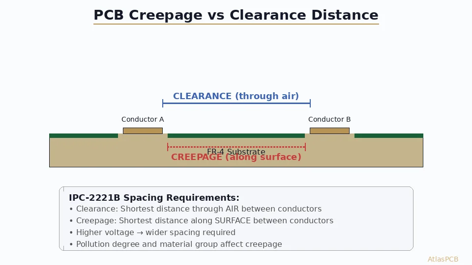
Clearance
The shortest distance through air between two conductive parts. Air can break down (arc) at approximately 1kV/mm under standard conditions.
Creepage
The shortest distance along the surface of insulation between two conductive parts. Surface tracking can occur at much lower voltages than air breakdown, especially with contamination or moisture.
Why Creepage > Clearance
Contamination (dust, flux residue, moisture) on PCB surfaces reduces the effective insulation. Surface tracking can propagate along contaminated paths at voltages far below the air breakdown voltage. Therefore, creepage distance requirements are always greater than clearance requirements.
Standards and Requirements
IEC 62368-1 (Audio/Video, IT Equipment)
Replaced IEC 60950-1 and IEC 60065. Defines safeguard requirements based on energy levels.
IEC 60601-1 (Medical Equipment)
Strictest requirements due to patient safety concerns. Requires MOPP (Means of Patient Protection).
Key Factors Determining Distance
- Working voltage: Higher voltage = greater distance required
- Pollution degree: PD1 (sealed), PD2 (normal indoor), PD3 (industrial)
- Material group: CTI (Comparative Tracking Index) of the PCB material
- Insulation type: Basic, supplementary, reinforced
Typical Creepage/Clearance (IEC 62368-1, PD2, Reinforced)
| Working Voltage (AC) | Clearance (min) | Creepage (min, Material III) |
|---|---|---|
| 120V | 2.5mm | 4.0mm |
| 240V | 4.0mm | 6.3mm |
| 400V | 5.5mm | 10.0mm |
PCB Design Techniques
Slots and Cutouts
When board space doesn’t allow sufficient surface distance, slots or cutouts in the PCB break the creepage path:
- A slot effectively increases creepage by forcing the path around it
- Minimum slot width: 0.5mm (some standards require 1.0mm)
- Slot must be completely through the board (no copper in slot walls)
- Creepage along a slot surface counts as 1x slot width per side
Guard Traces
A grounded trace between high and low voltage circuits:
- Adds creepage distance by breaking the direct path
- Must be connected to ground with multiple vias
- Width: 0.5-1.0mm typical
Board Edge Spacing
- High-voltage traces must be at least 5mm from board edges
- Board edges may have reduced creepage due to cutting roughness
- Solder mask coverage at edges may be incomplete
Layer Assignment
- Keep high-voltage traces on inner layers where possible
- Inner layer traces have no creepage concerns (encapsulated in laminate)
- Only outer layer traces need creepage/clearance compliance

Material Selection
CTI (Comparative Tracking Index)
CTI measures a material’s resistance to surface tracking. IPC standards group materials by CTI:
| Group | CTI Range | Examples |
|---|---|---|
| I | >= 600V | Special FR-4, Ceramic |
| II | 400-599V | High-grade FR-4 |
| IIIa | 175-399V | Standard FR-4 |
| IIIb | 100-174V | Low-grade materials |
Higher CTI = shorter required creepage distance. Using Group I material (CTI>=600V) can significantly reduce board size in high-voltage designs.
Board Thickness
- Thicker boards provide better through-board insulation
- Minimum 1.6mm for mains-voltage designs
- 2.0mm+ for medical or high-reliability applications
Isolation Barrier Design
Transformer Isolation (Most Common)
- Safety-rated transformer provides galvanic isolation
- PCB creepage/clearance maintained between primary and secondary windings on the board
- Optocouplers for feedback signal across isolation barrier
Capacitive Isolation
- Safety-rated Y capacitors bridge the isolation barrier
- Much smaller footprint than transformer
- Used in USB PD, isolated gate drivers
PCB Layout for Isolation
- Draw a clear isolation boundary line on the PCB
- Maintain required creepage/clearance across the entire boundary
- Use slots where the boundary crosses the PCB
- No copper pours or fills crossing the boundary
- Mark the boundary on silkscreen for visual inspection
- Route ground planes separately on each side of the barrier
Testing and Certification
Hi-Pot (Dielectric Withstand) Testing
- Apply test voltage between isolated circuits
- Typical: 2x working voltage + 1000V AC for 60 seconds
- Example: 240V AC mains → test at 1500V AC
- No breakdown or excessive leakage allowed
Safety Certification
- UL (United States): UL 62368-1
- CE (Europe): EN 62368-1
- CCC (China): GB 4943.1
- Each requires independent lab testing and certification
Conclusion
High-voltage PCB design is governed by safety standards that are non-negotiable. Understand the applicable standard for your product, calculate creepage and clearance requirements based on your specific voltage, pollution degree, and insulation type, and implement them rigorously in your layout. Use slots and guard traces to achieve required distances in compact designs. Verify with hi-pot testing before submitting for certification. Safety failures during certification testing are expensive — get the design right from the start.
Further Reading
[PCB Solder Mask: Types, Colors, and Functions Explained]/blog/pcb-solder-mask-guide/)
[IPC Class 3 Requirements: The Complete Guide for Designers]/blog/ipc-class-3-requirements/)
About AtlasPCB — We specialize in complex PCB manufacturing for HDI, RF, and high-reliability applications. Explore our full PCB manufacturing capabilities, or get an instant online quote . Every order includes free engineering review. Get your quote.
Reviewed by AtlasPCB Engineering Team — IPC-certified manufacturing specialists with 15+ years of production experience in HDI, RF, and high-reliability PCB fabrication. Content based on factory floor data and real customer design reviews.
- high voltage
- safety design
- creepage
- clearance