· AtlasPCB Engineering · Engineering · 6 min read
Siemens Fuse EDA AI Agent: How Autonomous Workflow Orchestration Is Changing PCB Design in 2026
Siemens' new Fuse EDA AI Agent brings autonomous multi-tool orchestration to PCB and semiconductor design. Explore how agentic AI with RAG, NVIDIA Nemotron, and physics-aware planning automates end-to-end EDA workflows — from schematic capture to manufacturing sign-off.
The Shift from AI Assistance to AI Autonomy in EDA
For the past five years, AI in electronic design automation has been limited to in-tool assistance: suggesting component placements, optimizing individual route segments, or flagging DRC violations. Useful, but still requiring engineers to manually orchestrate multi-step workflows between different tools.
Siemens’ announcement of the Fuse EDA AI Agent marks a fundamental transition: from AI that helps within a single tool to AI that autonomously manages entire design pipelines across multiple tools and teams.
This isn’t incremental improvement — it’s a category change. And it has profound implications for how PCBs get designed, validated, and released to manufacturing.
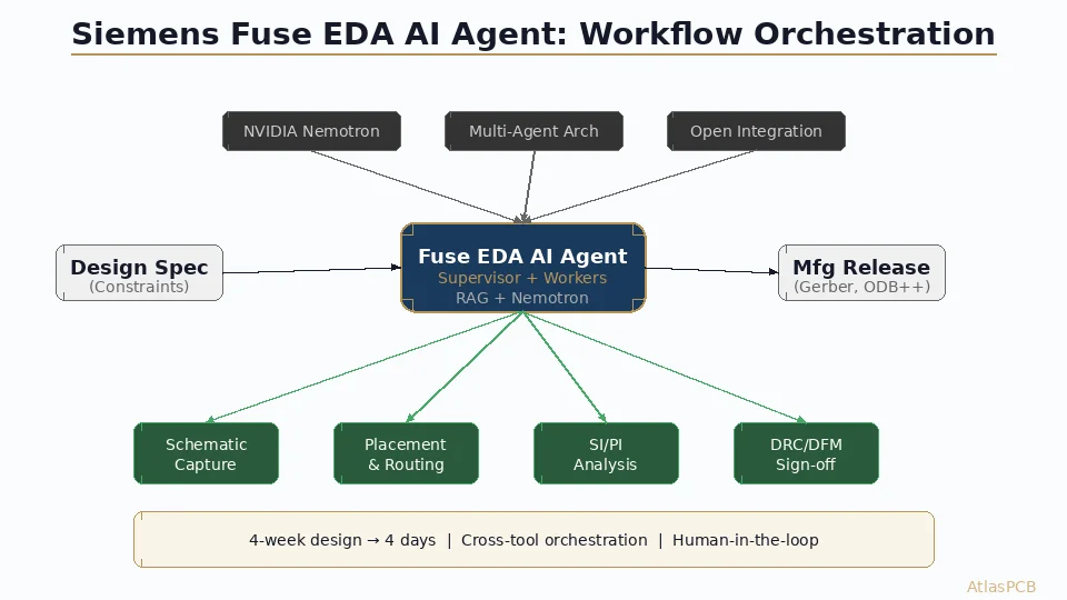
What Is the Fuse EDA AI Agent?
The Fuse EDA AI Agent is a domain-specific autonomous system built on several key technologies:
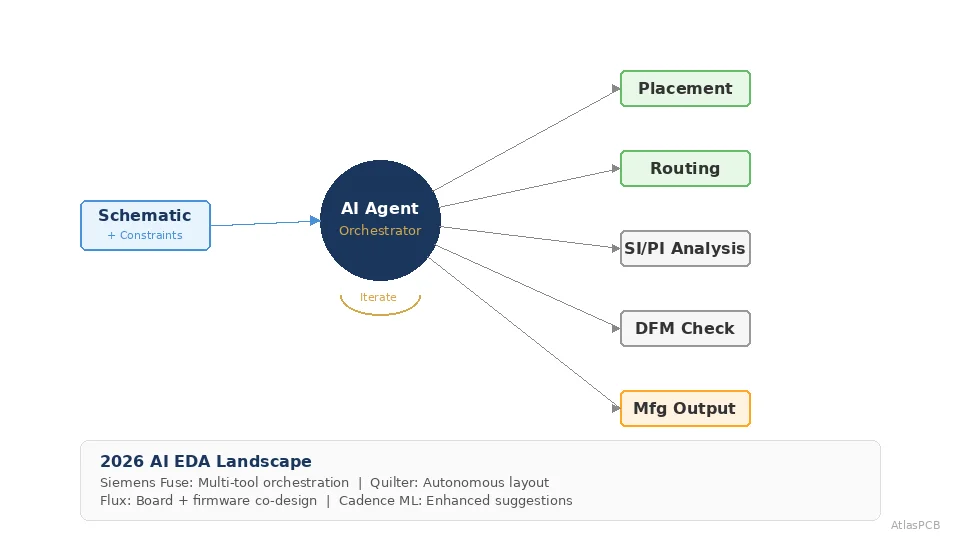
Multi-Agent Architecture
Rather than a single AI model trying to do everything, Fuse uses a hierarchical system:
- Supervisor agent: Decomposes complex design tasks into sub-tasks, allocates resources, monitors progress
- Worker agents: Specialized for specific domains (routing, verification, timing analysis)
- Orchestrator: Manages tool-to-tool data flow and dependency resolution
This mirrors how engineering teams actually work — a lead engineer coordinates specialists, each expert in their domain.
RAG with Physics-Aware Knowledge
The retrieval-augmented generation framework goes beyond generic LLM capabilities:
- Multimodal data processing: Understands schematics, layout images, waveform data, and text specifications simultaneously
- Domain knowledge base: Trained on EDA-specific documentation, design rules, and physics models
- Secure data governance: Enterprise-grade access control prevents sensitive IP from leaking between projects or organizations
NVIDIA Agent Toolkit Integration
Built on NVIDIA’s agent infrastructure:
- Nemotron models: Purpose-trained for engineering reasoning tasks
- AgentOps architecture: Scalable deployment across GPU clusters
- Dynamic tool orchestration: Real-time resource allocation for compute-intensive simulations
End-to-End Workflow Coverage
The agent covers the complete EDA lifecycle:
Front-End Design
- Architectural exploration and trade-off analysis
- Schematic capture assistance and netlist generation
- Testbench development for verification
- Block diagram to schematic translation
Physical Implementation
- Component placement optimization (thermal, signal integrity, manufacturing)
- Routing with multi-constraint awareness (impedance, timing, crosstalk)
- Timing closure and hold/setup margin optimization
- Power integrity analysis and decoupling strategy
Verification and Sign-Off
- Design rule checking (DRC) across all layers
- Electrical rule checking (ERC) for connectivity
- Signal integrity simulation (pre/post-layout)
- Manufacturing readiness validation (DFM/DFA)
- Gerber generation and release package preparation
The Critical Difference: Planning, Not Just Executing
Previous automation could execute individual steps when told to. The Fuse agent plans the sequence — deciding which analyses to run, when to iterate on a failing constraint, and how to prioritize conflicting requirements. It’s the difference between a robotic arm and a factory foreman.
Why This Matters for PCB Manufacturing
Manufacturing AI-Designed PCBs?
AtlasPCB's DFM review catches manufacturability issues before they reach the production floor — whether your design was human-created or AI-orchestrated.
Submit for DFM Review →Tighter Specifications, Higher Density
AI-optimized layouts tend to push closer to manufacturing limits:
- Trace/space: AI routing uses minimum clearances more aggressively than conservative human designers
- Via density: Automated placement fills available via locations for better signal return paths
- Layer utilization: Higher routing completion per layer means fewer layer count increases
- Impedance accuracy: AI can target tighter impedance windows (±5% vs. traditional ±10%)
For manufacturers, this means:
- Process capability must be documented and communicated accurately
- DFM feedback loops need to be faster (AI iterates in hours, not weeks)
- First-pass yield becomes more critical as designs leave less margin
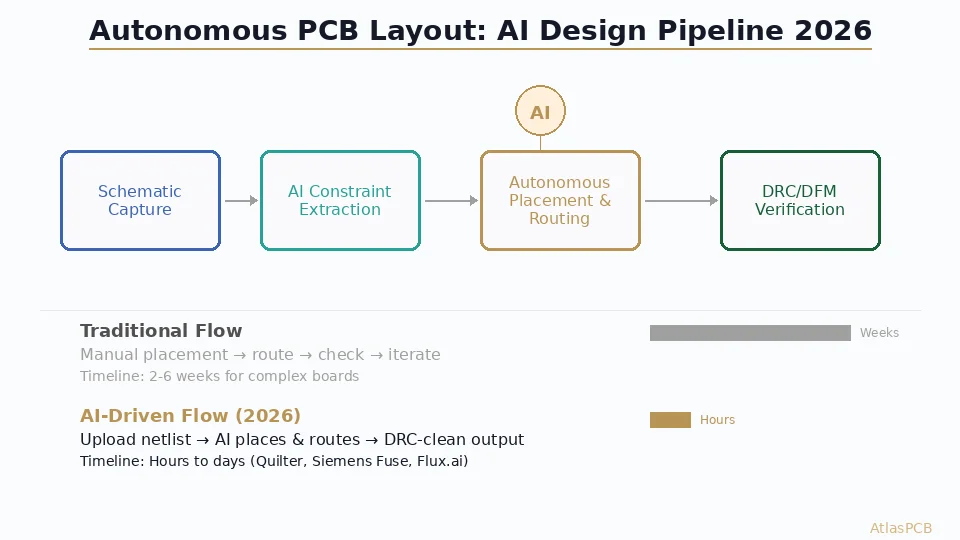
Compressed Design Cycles
When a PCB design that previously took 4 weeks compresses to 4 days through AI orchestration:
- Quote-to-production timelines shrink
- Prototype iteration speed increases dramatically
- Manufacturing partners must respond faster with quotes and DFM feedback
- Inventory and capacity planning becomes more dynamic
Data Format and Communication Changes
AI agents generate design data differently:
- Complete constraint files with every trace documented
- Automatic stackup proposals based on manufacturer capabilities
- Machine-readable DFM reports that AI can act on directly
- Potential for direct agent-to-MES communication in the future
Industry Collaboration: Samsung, NVIDIA, and Beyond
Siemens announced collaboration with major semiconductor companies:
- Samsung: Integrating Fuse into memory design workflows for cutting-edge semiconductor node development
- NVIDIA: Providing the underlying compute infrastructure and AI models
- Enterprise customers: Several undisclosed companies running pilot programs
The endorsement from Samsung is particularly significant — it validates that AI orchestration works for production-grade semiconductor and PCB system designs, not just demos.
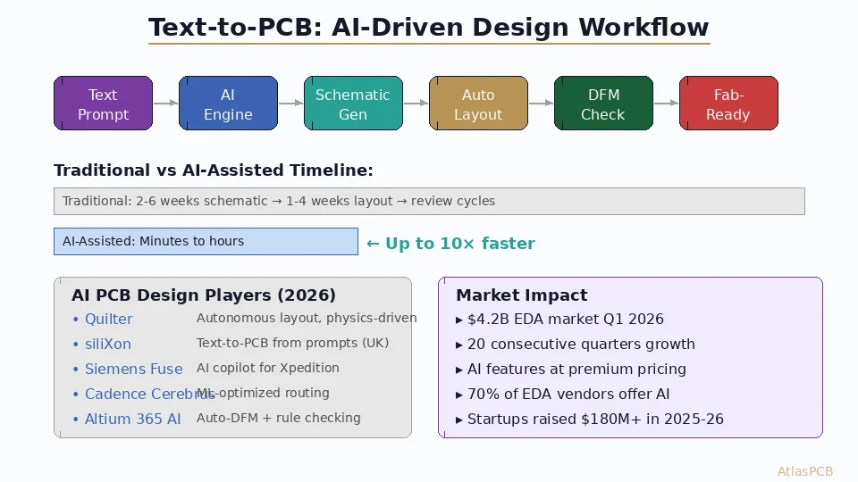
Competitive Landscape in AI EDA (2026)
Siemens isn’t alone in this space:
| Company | Product | Approach |
|---|---|---|
| Siemens | Fuse EDA AI Agent | Multi-agent orchestration, open architecture |
| Cadence | Cerebrus AI | Intelligent optimization within Cadence suite |
| Quilter | Autonomous Layout | Physics-first PCB auto-routing from scratch |
| Flux.ai | AI Copilot | Browser-based AI-assisted PCB design |
| Altium/Renesas | AI Features | In-tool assistance within Altium Designer |
The key differentiator for Siemens is the cross-tool orchestration — managing workflows across heterogeneous environments rather than optimizing within a single tool ecosystem.
Implications for Hardware Engineers
Skills That Become More Valuable
- System architecture — Defining what to build matters more when AI handles how to build it
- Constraint specification — Clearly articulating requirements in machine-readable formats
- Verification judgment — Knowing when AI results are trustworthy vs. need human review
- Manufacturing knowledge — Understanding what’s actually buildable at volume
Skills That Commoditize
- Routine placement and routing of standard circuits
- Manual DRC fixing of minor violations
- Repetitive schematic entry from reference designs
- Standard stackup selection for commodity boards
The “10× Engineer” Effect
Rather than replacing engineers, AI orchestration enables one experienced engineer to manage 5-10× more design projects simultaneously — setting up constraints and reviewing results rather than hand-routing every trace. This amplifies expertise rather than eliminating it.
What Comes Next
Near-Term (2026-2027)
- Wider enterprise deployment of agent-based workflows
- Integration with manufacturing execution systems (MES) for direct-to-fab handoff
- Specialized agents for domain verticals (automotive ADAS, 5G/6G infrastructure, medical)
Medium-Term (2028-2030)
- Agent-to-agent negotiation between design and manufacturing AI systems
- Continuous optimization of designs during production (digital twin feedback)
- Fully autonomous design of standard/commodity circuits from specification documents
Long-Term Questions
- How do you certify AI-designed circuits for safety-critical applications (ISO 26262, DO-254)?
- Who owns IP when AI generates novel circuit topologies?
- How do manufacturers validate designs they can’t fully trace the reasoning for?
What This Means for PCB Fabrication Partners
Manufacturers who adapt early will capture the wave:
- Publish machine-readable capabilities — Process parameters in standardized formats AI agents can consume
- Accelerate DFM turnaround — AI-designed boards arrive faster; slow quotes lose orders
- Invest in process capability — AI designs push limits; wider process windows win
- Build digital interfaces — API-based quoting and order submission for agent integration
- Document everything — Stackup options, material availability, lead times in structured data
Further Reading
- AI-Powered EDA Tools in 2026: Autonomous Agents Reshaping PCB Design
- Quilter AI Autonomous PCB Layout: From Speedrun to Production
- Siemens Xpedition Standard: AI PCB Design for SMBs
- IPC-2581 and the Smart Factory: AI Automation in PCB Manufacturing
Building boards for AI-accelerated design teams? AtlasPCB provides rapid DFM feedback, tight-tolerance manufacturing, and API-accessible quoting to keep pace with AI-driven design cycles. Get a quote or explore our capabilities.
About AtlasPCB — We specialize in complex PCB manufacturing for HDI, RF, and high-reliability applications. Explore our full PCB manufacturing capabilities, or get an instant online quote . Every order includes free engineering review. Get your quote.
Reviewed by AtlasPCB Engineering Team — IPC-certified manufacturing specialists with 15+ years of production experience in HDI, RF, and high-reliability PCB fabrication. Content based on factory floor data and real customer design reviews.
- AI PCB design
- Siemens Fuse
- EDA automation
- agentic AI
- PCB layout
- autonomous design
- machine learning