· Engineering · 7 min read
Immersion Silver vs OSP: Surface Finish Selection for High-Speed PCB Designs
Compare immersion silver and OSP surface finishes for high-speed digital and mixed-signal PCBs. Covers shelf life, solderability, signal integrity impact, cost, and decision criteria for choosing between these lead-free finishes.
Quick Answer: Immersion Silver vs OSP
| Parameter | Immersion Silver | OSP |
|---|---|---|
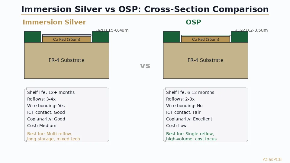
| Typical thickness | 0.15-0.40 um | 0.20-0.50 um |
| Shelf life (sealed) | 12+ months | 6-12 months |
| Reflow cycles | 3-4x | 2-3x (with re-application) |
| Coplanarity | Good | Excellent |
| Wire bonding | Yes (Au/Al) | No |
| ICT probe contact | Good | Fair (degrades with age) |
| Relative cost | Medium | Low |
| Lead-free compatible | Yes | Yes |
Bottom line: If your board sees multiple reflows or needs extended storage, use immersion silver. If cost is primary and you assemble within weeks of fabrication, OSP delivers equivalent solderability at lower cost.
Signal Integrity Comparison at the Pad Interface
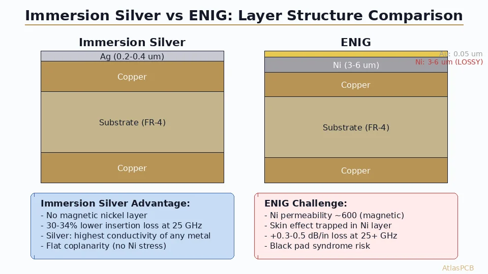
For high-speed designs operating above 5 GHz, surface finish selection affects insertion loss at component pad interfaces. Neither immersion silver nor OSP introduces significant signal degradation compared to ENIG, but there are measurable differences.
Immersion silver deposits a thin layer of pure silver (Ag) directly on copper. Silver has the highest electrical conductivity of any metal (6.3 x 10^7 S/m), so pad-to-trace transitions remain low-loss. The concern is tarnish: silver sulfide (Ag2S) forms when exposed to sulfur-containing atmospheres, creating resistive spots that degrade solderability but have minimal effect on high-frequency signal paths once the joint is formed.
OSP (Organic Solderability Preservative) applies a water-based organic compound (typically benzimidazole-based) that protects the underlying copper from oxidation. Since the OSP layer is consumed during soldering, the final joint is pure copper-to-solder — no intermediate metal layer. This means zero intermetallic concern at the pad, but the copper surface must remain uncontaminated.
For controlled impedance traces, neither finish affects the dielectric stack. The impact is limited to the solder pad and via landing geometry.
SURFACE FINISH ENGINEERING
Not Sure Which Finish Fits Your Design?
Our engineers review your Gerber files and recommend the optimal surface finish based on your assembly process, component mix, and reliability requirements.
Get a Recommendation ›Shelf Life and Storage: The Practical Differentiator
This is where the two finishes diverge most in practice.
Immersion Silver Storage
- Sealed in sulfur-free packaging: 12+ months
- After opening: 1-2 weeks in controlled environment (< 50% RH, < 25C)
- Anti-tarnish packaging required (sulfur-absorbing paper)
- No baking required before assembly
- Can survive warehouse storage for production builds with long lead times
OSP Storage
- Sealed with desiccant: 6-12 months (varies by OSP generation)
- After opening: 24-48 hours maximum before reflow
- Humidity sensitivity: Level 2 (per IPC J-STD-033)
- Requires nitrogen atmosphere during reflow for best results
- Second-generation OSP (high-temp OSP) extends reflow tolerance to 3 cycles
Real-world failure mode: Boards fabricated with OSP, shipped internationally, and stored in a non-climate-controlled warehouse for 3+ months will fail wetting tests. This is the single most common OSP-related assembly defect — not the finish itself, but logistics exposure.
If your supply chain involves any of these scenarios, immersion silver is the safer choice:
- Boards fabricated in Asia, assembled in North America/Europe
- Prototype builds where boards may sit on a shelf for weeks
- Consignment stock at a contract manufacturer
- Multi-phase assembly with weeks between top-side and bottom-side reflow
Assembly Process Compatibility
Single-Sided SMT (One Reflow)
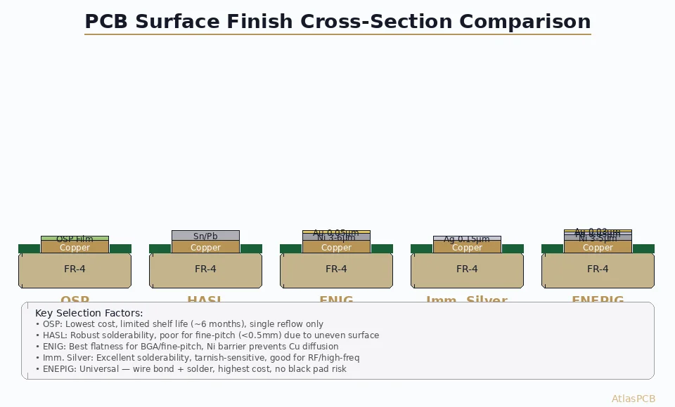
Both finishes perform identically. OSP is the cost-optimal choice here — it provides excellent wetting with SAC305 and SnPb solders, and coplanarity is best-in-class because there’s no metallic deposit creating pad height variation.
Double-Sided SMT (Two Reflows)
Immersion silver holds up better through the second reflow. OSP on the bottom side (which sees the first reflow inverted) partially degrades during the initial high-temperature exposure. The remaining OSP film may not provide adequate wetting for the second reflow pass.
Solutions for double-sided OSP boards:
- Use nitrogen atmosphere during second reflow (reduces oxidation)
- Specify high-temperature OSP formulation (withstands 260C peak 3x)
- Ensure second reflow occurs within 4 hours of the first
Mixed Technology (SMT + Wave/Selective Solder)
Immersion silver is preferred. The wave soldering flux activation can strip residual OSP inconsistently, leading to skip soldering on through-hole pins. Silver maintains solderable surfaces through the entire process sequence.
PRODUCTION-READY BOARDS
Both Finishes, Same Lead Time
AtlasPCB processes immersion silver and OSP on dedicated lines. Upload your design and select your preferred finish — or let us recommend based on your BOM and assembly flow.
Upload Gerber Files ›ICT and Functional Test Considerations
In-circuit test (ICT) probes make direct contact with test pads. Surface finish affects probe contact reliability over the board’s test life:
Immersion silver: Consistent probe contact. Silver surface provides low contact resistance even after moderate tarnish. Probe marks are minimal and don’t compromise subsequent soldering if rework is needed.
OSP: Fresh OSP boards test well. Boards that have been in storage or partially oxidized show intermittent probe contact failures, especially at fine-pitch test points (< 0.5mm diameter pads). The organic film can create variable contact resistance.
If your production flow requires 100% ICT with boards that may wait hours or days between fabrication and testing, immersion silver reduces false test failures.
Cost Analysis Per Panel
For a typical 4-layer board on a standard 18x24” production panel:
| Cost Factor | Immersion Silver | OSP |
|---|---|---|
| Chemistry cost/panel | $3.50-5.00 | $1.50-2.50 |
| Process time | 8-12 min | 3-5 min |
| Line utilization | Medium | High |
| Waste treatment | Silver recovery required | Minimal waste |
| Typical adder vs bare Cu | $4-6/panel | $2-3/panel |
At production volumes (1000+ panels), the cost gap is approximately $2-4 per panel. For a 10-up panel (10 boards per panel), that translates to $0.20-0.40 per board — often negligible compared to component costs but significant at very high volumes (100K+ boards/year).
COMPARE YOUR OPTIONS
Get Pricing for Both Finishes
Upload your design once — receive quotes with immersion silver and OSP options side by side. See exactly how surface finish choice affects your per-board cost.
Compare Prices ›Decision Framework
Choose OSP when:
- Single reflow, single-sided assembly
- High-volume production with short fab-to-assembly cycle (< 2 weeks)
- Cost reduction is a priority
- Fine-pitch BGA requiring best pad coplanarity
- No ICT testing, or testing occurs same day as fab
Choose Immersion Silver when:
- Double-sided or multi-step assembly process
- Boards stored > 2 weeks before assembly
- International shipping between fab and assembly
- Mixed technology (SMT + wave solder)
- ICT testing required
- Wire bonding on any pads
- Customer specifies per IPC-4553 (Immersion Silver)
Consider ENIG instead when:
- You need both wire bonding AND long shelf life AND multiple reflows
- Fine-pitch QFN with exposed pad (ENIG’s nickel barrier prevents copper dissolution)
- Design requires gold-to-gold contact surfaces (connectors, test points)
For more on ENIG and its comparison with silver finishes, see our detailed guide on immersion silver vs ENIG for high-reliability applications.
ATLASPCB
Ready to Order? We Support All Major Surface Finishes
OSP, immersion silver, ENIG, immersion tin, HASL, and hard gold — all processed in-house with IPC Class 2/3 quality standards.
Get Instant Quote ›Related Reading:
About AtlasPCB — We specialize in complex PCB manufacturing for HDI, RF, and high-reliability applications. Explore our RF and high-frequency PCB services, or get an impedance-controlled PCB manufacturing . Every order includes free engineering review. Get your quote.
Reviewed by AtlasPCB Engineering Team — IPC-certified manufacturing specialists with 15+ years of production experience in HDI, RF, and high-reliability PCB fabrication. Content based on factory floor data and real customer design reviews.
- surface-finish
- high-speed-pcb
- immersion-silver
- osp
- signal-integrity