· Marcus Lin · Engineering · 7 min read
Selective Surface Finish on PCB
Learn how to specify multiple surface finishes on a single PCB for optimal cost and performance. Covers process sequencing, masking techniques, DFM rules, and real-world applications in connector, RF, and mixed-technology designs.
Quick Answer
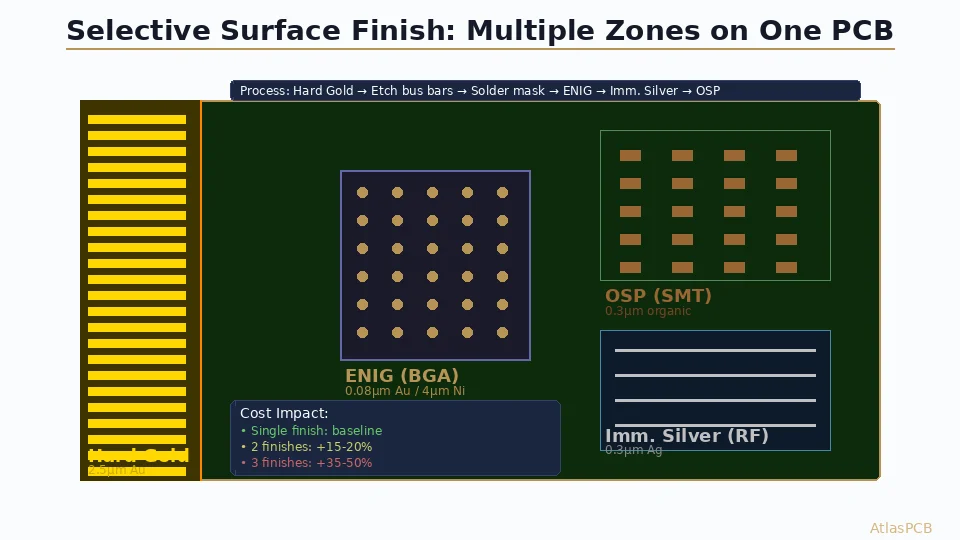
Selective surface finish applies different metal coatings to different areas of the same PCB — for example, hard gold on edge connector fingers for wear resistance, ENIG on fine-pitch BGA pads for solderability and coplanarity, and OSP on standard SMT pads for lowest cost. This requires careful process sequencing (hard gold first → ENIG second → OSP last) and precise masking (photoresist or tape) to prevent cross-contamination between finish zones.
Introduction: One Board, Multiple Demands
Modern PCB designs rarely have uniform requirements across all exposed copper surfaces. A single board may include:
- Edge connector fingers that endure 500+ mating cycles (needs hard gold)
- Fine-pitch BGA pads requiring perfect coplanarity (needs ENIG or ENEPIG)
- RF transmission lines demanding lowest insertion loss (needs immersion silver)
- Standard SMT pads for commodity passives (cost-effective OSP suffices)
- Wire bond pads requiring soft gold for thermosonic bonding
- Press-fit holes needing bare copper for compliant pin retention
Applying a single surface finish forces compromise: ENIG everywhere is expensive and suboptimal for RF; OSP everywhere fails for connectors and BGA coplanarity; hard gold everywhere is prohibitively expensive and can cause solder embrittlement.
Selective surface finish solves this by applying the right finish to each functional zone. This guide covers the engineering and manufacturing process behind multi-finish PCBs.
Available Finish Types and Their Strengths
Quick Reference: Finish Properties
| Finish | Thickness | Shelf Life | Solder | Wear | RF Loss | Cost |
|---|---|---|---|---|---|---|
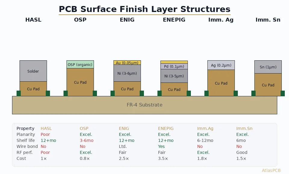
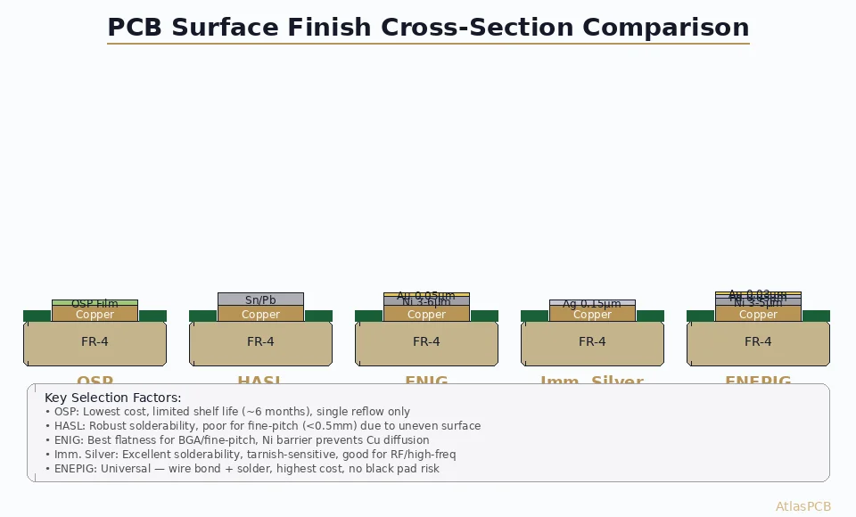
| OSP | 0.2–0.5 μm | 6 months | Excellent | None | Good | Lowest |
| ENIG | Ni 3–5 μm + Au 0.05–0.1 μm | 12+ months | Very Good | Low | Fair | Medium |
| ENEPIG | Ni 3–5 + Pd 0.05–0.15 + Au 0.05 μm | 12+ months | Excellent | Low | Fair | High |
| Immersion Silver | 0.15–0.4 μm | 6–12 months | Excellent | None | Excellent | Medium |
| Immersion Tin | 0.8–1.2 μm | 6 months | Excellent | None | Good | Low-Med |
| Hard Gold (electrolytic) | Ni 3–5 μm + Au 0.75–2.5 μm | Indefinite | Good* | Excellent | Poor | Highest |
*Hard gold requires removal from solder areas (gold embrittlement risk above 3% Au in joint)
When Each Finish Excels
OSP (Organic Solderability Preservative):
- Cost-optimized SMT pads
- Best wetting for Pb-free solder
- Flush, ultra-flat surface (< 1 μm variation)
- Limitation: moisture-sensitive, single reflow only recommended
ENIG (Electroless Nickel/Immersion Gold):
- Fine-pitch BGA (≤ 0.5 mm) — coplanarity critical
- Mixed technology (SMT + wave solder + press-fit on same board)
- Long shelf life requirements (12+ months before assembly)
- Al wire bonding capability
Hard Gold (Electrolytic Nickel/Gold):
- Edge connectors (PCIe, DIMM, card-edge)
- Test points for spring-loaded probes (pogo pins)
- Switch contacts and sliding surfaces
- Specification: IPC-4552 Type III, 0.75–2.5 μm gold over 2.5–5.0 μm nickel
Immersion Silver:
- RF/microwave traces (lowest skin-effect loss after bare copper)
- EMI shielding surfaces
- High-frequency antenna elements
- Limitation: tarnish-sensitive, requires nitrogen storage
Process Sequencing: Order Matters
The fundamental challenge of selective finishing is that each process involves wet chemistry that must not contaminate other finish zones. The standard sequence follows a “most aggressive first” principle:
Recommended Process Order
1. Electrolytic Hard Gold (requires bus bars, done before final etch)
2. Final copper pattern etch (removes bus bars)
3. Solder mask application
4. Masking for selective ENIG/ENEPIG
5. ENIG/ENEPIG process on exposed zones
6. Strip mask from remaining zones
7. Apply OSP or Immersion Silver to remaining pads
Why Hard Gold Must Come First
Hard gold is an electrolytic process requiring electrical connection (bus bars) from a common plating bus to every gold-plated feature. These bus bars are part of the copper pattern and are etched away during circuit definition. This makes hard gold a pre-etch process — it must happen before the final copper pattern is defined.
After hard gold plating:
- Bus bars are etched (breaking electrical connections)
- Solder mask is applied (protecting hard gold areas from subsequent chemistry)
- Chemical finishes (ENIG, immersion silver, OSP) are applied selectively
Masking Technologies
Photoresist Masking (Precision):
- Dry film photoresist applied and exposed over areas to protect
- Accuracy: ±0.05 mm registration
- Used when finish zones are close together (< 2 mm spacing)
- Stripped after process step completes
Tape Masking (Economical):
- Kapton or chemical-resistant tape manually or die-cut applied
- Accuracy: ±0.5 mm (adequate for separated zones)
- Used for large area protection (e.g., connector vs. rest of board)
- Fast and inexpensive for simple geometries
Solder Mask as Mask:
- The solder mask itself protects covered areas
- Only exposed pads receive the surface finish
- No additional masking needed when solder mask openings define finish zones
Design Rules for Selective Finishing
Zone Separation Requirements
The minimum spacing between different finish zones depends on the masking method:
| Finish Combination | Min Spacing (Photoresist) | Min Spacing (Tape) |
|---|---|---|
| Hard Gold ↔ ENIG | 0.5 mm | 2.0 mm |
| ENIG ↔ OSP | 0.3 mm | 1.5 mm |
| ENIG ↔ Imm Silver | 0.5 mm | 2.0 mm |
| Hard Gold ↔ OSP | 0.5 mm | 2.0 mm |
DFM Guidelines
- Define finish zones clearly in fabrication drawing — include zone boundaries with finish callouts
- Avoid finish transitions under components — place zone boundaries in solder-mask-covered areas
- Account for plating thickness in impedance calculations — 5 μm Ni under hard gold affects trace impedance
- Specify gold thickness removal from solder pads — if hard gold bus bars route through SMT pad areas, gold must be etched back before ENIG application
- Include test coupons for each finish — solder spread test, adhesion test, thickness verification
Gerber/Fabrication Data
In addition to standard Gerber layers, selective finish requires:
- Finish zone layer (custom Gerber or mechanical layer) defining each finish area
- Finish specification table in fabrication notes
- Bus bar layer (if hard gold) showing plating connections
Multi-Finish PCB Manufacturing
AtlasPCB handles up to 3 selective finishes on one board with photoresist-level precision. Hard gold + ENIG + OSP delivered in 10 working days.
Get Multi-Finish Quote →Common Selective Finish Combinations
Combination 1: Hard Gold + ENIG (Most Common)
Application: PCIe card, DIMM module, any board with edge connector + BGA
Design:
- Edge connector fingers: Hard gold (1.27 μm Au / 3.8 μm Ni), IPC-4552 Class 3
- BGA/SMT pads: ENIG (0.08 μm Au / 4.0 μm Ni)
- Zone boundary: At solder mask dam between connector and first SMT pad row (typically 2–3 mm)
Process notes:
- Hard gold applied before circuit etch
- ENIG chemistry does not attack existing hard gold (Ni barrier intact)
- Cost premium vs. all-ENIG: approximately +15%
Combination 2: ENIG + OSP (Cost Optimized)
Application: BGA device with standard SMT passives, telecom equipment
Design:
- BGA pads, QFP pads: ENIG (coplanarity and shelf life critical)
- Standard 0402/0603 passive pads: OSP (lowest cost, best wetting)
- Zone boundary: Solder mask defines zones naturally
Process notes:
- ENIG applied first with photoresist mask over OSP areas
- OSP applied to remaining exposed copper after mask strip
- Cost saving vs. all-ENIG: approximately -20%
Combination 3: Hard Gold + Immersion Silver + OSP
Application: RF transceiver with card-edge connector
Design:
- Connector fingers: Hard gold (wear resistance)
- RF traces, antenna elements: Immersion silver (lowest RF loss)
- Digital SMT pads: OSP (cost optimized)
Process notes:
- Most complex combination requiring 3 masking/processing cycles
- Silver must be the last chemical finish (most sensitive to contamination)
- Requires nitrogen packaging after final finish
- Cost premium vs. single finish: approximately +40%
Combination 4: ENEPIG + Immersion Silver
Application: Mixed die-attach (wire bond) and RF board
Design:
- Wire bond pads: ENEPIG (gold wire and aluminum wire compatible)
- RF transmission lines: Immersion silver
- Other SMT: ENEPIG (already applied)
Process notes:
- ENEPIG’s palladium layer provides gold wire bond reliability
- Silver applied selectively only on RF-critical paths
- Excellent combination for 5G antenna-in-package substrate
Quality Control and Inspection
Thickness Verification
Each finish zone requires independent thickness measurement:
- XRF (X-ray Fluorescence): Non-destructive, measures each layer independently
- Cross-section: Destructive, confirms plating uniformity and adhesion
- Beta backscatter: Fast screening for gold thickness on connectors
Adhesion Testing
- Tape pull test (ASTM D3359): All finish types, checks delamination risk
- Solder spread test: Verifies wettability on OSP and ENIG zones
- Insertion/withdrawal force: Connector-specific hard gold validation
Common Defects
| Defect | Cause | Prevention |
|---|---|---|
| Gold bleed into ENIG zone | Mask undercut during plating | Tighter photoresist exposure |
| OSP in ENIG areas | Incomplete mask strip | Verify strip with UV inspection |
| Nickel skip-plating | Surface contamination | Microetch before each finish |
| Silver tarnish | Handling without gloves | Nitrogen storage, gloved handling |
Cost Impact Analysis
Additional Cost Factors
Each selective finish adds:
- Masking material and application: $0.50–2.00 per board
- Additional wet processing step: $1.00–3.00 per board
- Extra inspection cycle: $0.25–1.00 per board
- Yield loss from masking defects: 1–3% per masking step
Break-Even Analysis
For a typical 150 × 100 mm board:
- All ENIG: baseline cost $X
- Hard Gold + ENIG: $X + 15–20%
- ENIG + OSP (selective): $X - 10–20% (OSP areas save material)
- Hard Gold + ENIG + OSP: $X + 25–35%
- Triple selective (HG + ENIG + Imm Ag): $X + 35–50%
The cost increase is justified when functional requirements demand it — no single finish can match hard gold’s 500-cycle connector durability AND ENIG’s BGA coplanarity AND silver’s RF performance.
Advanced Applications
5G mmWave Modules
5G antenna-in-package modules often require:
- Immersion silver on antenna array (28/39 GHz, loss-critical)
- ENEPIG on flip-chip pads (die attach reliability)
- Hard gold on board-to-board connector
- Three selective finishes on a 30 × 30 mm substrate
Automotive Radar (77 GHz)
Automotive radar PCBs increasingly use:
- Immersion silver on microstrip feed network (minimize loss at 77 GHz)
- ENIG on digital/power SMT pads (automotive shelf life requirements)
- Zone boundary at transition from RF substrate to digital substrate in hybrid stackup
Medical Implantable Devices
- Hard gold on hermetic connector pins (biocompatibility + wear)
- ENIG on internal assembly pads (solderability)
- Custom specification for implant-grade cleanliness (< 0.5 μg/cm² ionic)
Further Reading
- PCB Surface Finish Comparison 2026: ENIG, HASL, OSP, Hard Gold, ENEPIG
- ENIG vs ENEPIG Surface Finish Selection Guide
- PCB Gold Finger Connector Design Guide
- mmWave PCB Material Selection: Rogers, Megtron, and LCP
Need a multi-finish PCB with hard gold connectors, ENIG BGA pads, and optimized RF surfaces? AtlasPCB’s selective finishing process handles up to 3 finish types with photoresist-level precision. Request a quote with your finish zone requirements.
About AtlasPCB — We specialize in complex PCB manufacturing for HDI, RF, and high-reliability applications. Explore our RF and high-frequency PCB services, free engineering DFM review, or get an full PCB manufacturing capabilities . Every order includes free engineering review. Get your quote.
Reviewed by AtlasPCB Engineering Team — IPC-certified manufacturing specialists with 15+ years of production experience in HDI, RF, and high-reliability PCB fabrication. Content based on factory floor data and real customer design reviews.
Frequently Asked Questions
What is the maximum number of different surface finishes on one PCB?
Can ENIG and hard gold coexist on the same board without galvanic compatibility issues?
Why not just use ENIG everywhere instead of selective finishes?
- surface finish
- ENIG
- hard gold
- OSP
- immersion silver
- selective plating
- PCB manufacturing
- DFM